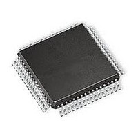
ST92T163R4T1 STMicroelectronics, ST92T163R4T1 Datasheet - Page 103

ST92T163R4T1
Manufacturer Part Number
ST92T163R4T1
Description
Microcontrollers (MCU) OTP EPROM 20K USB/I2
Manufacturer
STMicroelectronics
Datasheet
1.ST92T163R4T1.pdf
(224 pages)
Specifications of ST92T163R4T1
Data Bus Width
8 bit, 16 bit
Program Memory Type
EPROM
Program Memory Size
20 KB
Data Ram Size
2 KB
Interface Type
I2C, SCI, USB
Maximum Clock Frequency
24 MHz
Number Of Programmable I/os
64
Number Of Timers
2
Operating Supply Voltage
4 V to 5.5 V
Maximum Operating Temperature
+ 70 C
Mounting Style
SMD/SMT
Package / Case
TQFP-64
Minimum Operating Temperature
0 C
On-chip Adc
8 bit
Lead Free Status / Rohs Status
No
Available stocks
Company
Part Number
Manufacturer
Quantity
Price
Company:
Part Number:
ST92T163R4T1L
Manufacturer:
ST
Quantity:
444
Part Number:
ST92T163R4T1L
Manufacturer:
ST
Quantity:
20 000
7.5 ALTERNATE FUNCTION ARCHITECTURE
Each I/O pin may be connected to three different
types of internal signal:
– Data bus Input/Output
– Alternate Function Input
– Alternate Function Output
7.5.1 Pin Declared as I/O
A pin declared as I/O, is connected to the I/O buff-
er. This pin may be an Input, an Output, or a bidi-
rectional I/O, depending on the value stored in
(PxC2, PxC1 and PxC0).
7.5.2 Pin Declared as an Alternate Input
A single pin may be directly connected to several
Alternate inputs. In this case, the user must select
the required input mode (with the PxC2, PxC1,
PxC0 bits) and enable the selected Alternate
Function in the Control Register of the peripheral.
No specific port configuration is required to enable
an Alternate Function input, since the input buffer
is directly connected to each alternate function
module on the shared pin. As more than one mod-
ule can use the same input, it is up to the user soft-
ware to enable the required module as necessary.
Parallel I/Os remain operational even when using
an Alternate Function input. The exception to this
is when an I/O port bit is permanently assigned by
hardware as an A/D bit. In this case , after soft-
ware programming of the bit in AF-OD-TTL, the Al-
ternate function output is forced to logic level 1.
The analog voltage level on the corresponding pin
is directly input to the A/D.
7.5.3 Pin Declared as an Alternate Function
Output
The user must select the AF OUT configuration
using the PxC2, PxC1, PxC0 bits. Several Alter-
nate Function outputs may drive a common pin. In
such case, the Alternate Function output signals
are logically ANDed before driving the common
pin. The user must therefore enable the required
Alternate Function Output by software.
WARNING: When a pin is connected both to an al-
ternate function output and to an alternate function
input, it should be noted that the output signal will
always be present on the alternate function input.
7.6 I/O STATUS AFTER WFI, HALT AND RESET
The status of the I/O ports during the Wait For In-
terrupt, Halt and Reset operational modes is
shown in the following table. The External Memory
Interface ports are shown separately. If only the in-
ternal memory is being used and the ports are act-
ing as I/O, the status is the same as shown for the
other I/O ports.
RESET
Mode
HALT
WFI
address (de-
High Imped-
ance or next
High Imped-
memory op-
Alternate function push-
pull (ROMless device)
eration per-
pending on
formed on
Ext. Mem - I/O Ports
the last
Port)
ance
P0
P1, P2, P6
Address
Address
Next
Next
ST92163 - I/O PORTS
Not Affected (clock
outputs running)
Not Affected (clock
outputs stopped)
Bidirectional Weak
Pull-up (High im-
pedance when disa-
bled in hardware).
I/O Ports
103/224


