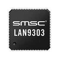
LAN9303-ABZJ SMSC, LAN9303-ABZJ Datasheet - Page 30

LAN9303-ABZJ
Manufacturer Part Number
LAN9303-ABZJ
Description
IC ETHER SW 3PORT 16BIT 56QFN
Manufacturer
SMSC
Specifications of LAN9303-ABZJ
Controller Type
Ethernet Switch Controller
Interface
SMBus (2-Wire/I²C)
Voltage - Supply
3 V ~ 3.6 V
Current - Supply
190mA
Operating Temperature
0°C ~ 70°C
Mounting Type
Surface Mount
Package / Case
56-QFN
Product
Ethernet Switches
Standard Supported
Yes
Data Rate
10 Mbps/100 Mbps
Supply Voltage (max)
3.6 V
Supply Voltage (min)
3 V
Supply Current (max)
0.19 A (Typ)
Maximum Operating Temperature
+ 70 C
Minimum Operating Temperature
0 C
Mounting Style
SMD/SMT
For Use With
638-1095 - EVALUATION BOARD FOR LAN9303
Lead Free Status / Rohs Status
Lead free / RoHS Compliant
Other names
638-1082
Available stocks
Company
Part Number
Manufacturer
Quantity
Price
Part Number:
LAN9303-ABZJ
Manufacturer:
MICROCHIP/微芯
Quantity:
20 000
- Current page: 30 of 367
- Download datasheet (4Mb)
Revision 1.4 (07-07-10)
PINS
NUM
1
1
Reference
Port 0 MII
Port 0 MII
Collision
NAME
Output
Clock
P0_OUTCLK
SYMBOL
P0_COL
Table 3.4 Port 0 MII/RMII Pins (continued)
Small Form Factor Three Port 10/100 Managed Ethernet Switch with Single MII/RMII/Turbo MII
DATASHEET
BUFFER
O12/O16
IS/O12/
TYPE
(PD)
(PD)
(PU)
O16
O8
IS
IS
-
30
MII MAC Mode: This pin is an input and is used as
the reference clock for the P0_OUTD[3:0] and
P0_OUTDV pins. It is connected to the transmit
clock of the external PHY.
MII PHY Mode: This pin is an output and is used
as the reference clock for the P0_OUT[3:0] and
P0_OUTDV pins. It is connected to the receive
clock of the external MAC. The output driver is
disabled when the
the
(VPHY_BASIC_CTRL). When operating at
200MBps, the choice of drive strength is based on
the setting of the
in the
(VPHY_SPECIAL_CONTROL_STATUS). A low
selects a 12 mA drive, while a high selects a 16 mA
drive. A series terminating resistor is recommended
for the best PCB signal integrity.
RMII PHY Mode: This pin is an input or an output
running at 50 MHz and is used as the reference
clock for the P0_IND[1:0], P0_INDV,
P0_OUTD[1:0], and P0_OUTDV pins. The choice
of input verses output is based on the setting of the
RMII Clock Direction
Control/Status Register
(VPHY_SPECIAL_CONTROL_STATUS). A low
selects P0_OUTCLK as an input and a high selects
P0_OUTCLK as an output.
As an input, the pull-down is normally enabled. The
input buffer and pull-down are disabled when the
Isolate (VPHY_ISO)
Basic Control Register
As an output, the input buffer and pull-down are
disabled. The choice of drive strength is based on
the MII Virtual PHY
bit. A low selects a 12 mA drive, while a high
selects a 16 mA drive. The output driver is disabled
when the
Virtual PHY Basic Control Register
(VPHY_BASIC_CTRL). A series terminating
resistor is recommended for the best PCB signal
integrity.
MII MAC Mode: This pin is an input from the
external PHY and indicates a collision event.
MII PHY Mode: This pin is an output to the external
MAC indicating a collision event. The output driver
is disabled when the
in the
(VPHY_BASIC_CTRL).
RMII PHY Mode: This pin is not used.
Virtual PHY Basic Control Register
Virtual PHY Special Control/Status Register
Virtual PHY Basic Control Register
Isolate (VPHY_ISO)
RMII/Turbo MII Clock Strength
DESCRIPTION
Isolate (VPHY_ISO)
RMII/Turbo MII Clock Strength
bit is set in the
Isolate (VPHY_ISO)
bit in the
(VPHY_BASIC_CTRL).
SMSC LAN9303/LAN9303i
Virtual PHY Special
bit is set in the
Virtual PHY
bit is set in
bit is set
Datasheet
bit
Related parts for LAN9303-ABZJ
Image
Part Number
Description
Manufacturer
Datasheet
Request
R

Part Number:
Description:
FAST ETHERNET PHYSICAL LAYER DEVICE
Manufacturer:
SMSC Corporation
Datasheet:

Part Number:
Description:
357-036-542-201 CARDEDGE 36POS DL .156 BLK LOPRO
Manufacturer:
SMSC Corporation
Datasheet:

Part Number:
Description:
357-036-542-201 CARDEDGE 36POS DL .156 BLK LOPRO
Manufacturer:
SMSC Corporation
Datasheet:

Part Number:
Description:
357-036-542-201 CARDEDGE 36POS DL .156 BLK LOPRO
Manufacturer:
SMSC Corporation
Datasheet:

Part Number:
Description:
4-PORT USB2.0 HUB CONTROLLER
Manufacturer:
SMSC Corporation
Datasheet:

Part Number:
Description:
Manufacturer:
SMSC Corporation
Datasheet:

Part Number:
Description:
Manufacturer:
SMSC Corporation
Datasheet:

Part Number:
Description:
FDC37C672ENHANCED SUPER I/O CONTROLLER WITH FAST IR
Manufacturer:
SMSC Corporation
Datasheet:

Part Number:
Description:
COM90C66LJPARCNET Controller/Transceiver with AT Interface and On-Chip RAM
Manufacturer:
SMSC Corporation
Datasheet:

Part Number:
Description:
Manufacturer:
SMSC Corporation
Datasheet:

Part Number:
Description:
Manufacturer:
SMSC Corporation
Datasheet:

Part Number:
Description:
Manufacturer:
SMSC Corporation
Datasheet:

Part Number:
Description:
Manufacturer:
SMSC Corporation
Datasheet:


