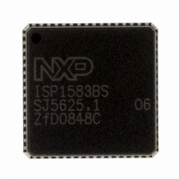
ISP1583BSUM ST-Ericsson Inc, ISP1583BSUM Datasheet - Page 84

ISP1583BSUM
Manufacturer Part Number
ISP1583BSUM
Description
IC USB PERIPH CONTROLLER 64HVQFN
Manufacturer
ST-Ericsson Inc
Datasheet
1.ISP1583BSUM.pdf
(100 pages)
Specifications of ISP1583BSUM
Controller Type
USB Peripheral Controller
Interface
Parallel/Serial
Voltage - Supply
3 V ~ 3.6 V
Current - Supply
47mA
Operating Temperature
-40°C ~ 85°C
Mounting Type
Surface Mount
Package / Case
64-VQFN Exposed Pad, 64-HVQFN, 64-SQFN, 64-DHVQFN
Lead Free Status / RoHS Status
Lead free / RoHS Compliant
Other names
568-1886-2
ISP1583BS,518
ISP1583BS-T
ISP1583BS,518
ISP1583BS-T
Available stocks
Company
Part Number
Manufacturer
Quantity
Price
Company:
Part Number:
ISP1583BSUM
Manufacturer:
MICRON
Quantity:
2 000
Company:
Part Number:
ISP1583BSUM
Manufacturer:
ST-ERICS
Quantity:
829
Part Number:
ISP1583BSUM
Manufacturer:
STE
Quantity:
20 000
NXP Semiconductors
Table 110. MDMA mode timing parameters
V
[1]
ISP1583_7
Product data sheet
Symbol
T
t
t
t
t
t
t
t
t
t
t
w1(min)
d1(max)
h3(min)
su2(min)
h2(min)
su1(min)
h1(min)
w2(min)
d2(max)
d3(max)
CC(I/O)
Fig 35. MDMA master mode timing
cy1(min)
T
Minimum timing requirements for T
implementation must lengthen t
data. A device implementation shall support any legal host implementation.
cy1
(write) DATA [ 15:0 ]
(1) Programmable polarity: shown as active LOW.
(2) Programmable polarity: shown as active HIGH.
(read) DATA [ 15:0 ]
DIOR or DIOW
= 1.65 V to 3.6 V; V
is the total cycle time, consisting of command active time t
DREQ
DACK
Parameter
read/write cycle time
DIOR or DIOW pulse width
data valid delay after DIOR on
data hold time after DIOR off
data set-up time before DIOR or DIOW off
data hold time after DIOW off
DACK set-up time before DIOR or DIOW on
DACK hold time after DIOR or DIOW off
DIOR recovery time
DIOW recovery time
DIOR on to DREQ off delay
DIOW on to DREQ off delay
DACK off to data lines 3-state delay
13.2.3 MDMA mode
(2)
(1)
(1)
t
su1
CC(3V3)
w1
t
d1
= 3.3 V; V
and/or t
cy1
, t
w1
t
w1
w2
and t
t
su2
to ensure that T
GND
w2
Rev. 07 — 22 September 2008
must all be met. As T
= 0 V; T
t
h3
amb
cy1
w1
Conditions
= 40 C to +85 C; unless otherwise specified.
is equal to or greater than the value reported in the IDENTIFY DEVICE
t
w2
and command recovery (inactive) time t
cy1(min)
T
cy1
is greater than the sum of t
[1]
[1]
[1]
[1]
Mode 0
480
215
150
5
100
20
0
20
50
215
120
40
20
Hi-Speed USB peripheral controller
t
d2
t
su2
Mode 1
150
80
60
5
30
15
0
5
50
50
40
40
25
t
h1
w2
w1(min)
, that is, T
t
t
h2
d3
Mode 2
120
70
50
5
20
10
0
5
25
25
35
35
25
© NXP B.V. 2008. All rights reserved.
and t
ISP1583
cy1
w2(min)
= t
mgt506
w1
, a host
Unit
ns
ns
ns
ns
ns
ns
ns
ns
ns
ns
ns
ns
ns
+ t
83 of 99
w2
.


