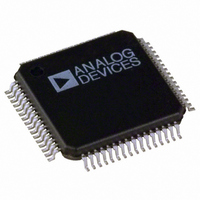
ADE7166ASTZF8 Analog Devices Inc, ADE7166ASTZF8 Datasheet - Page 99

ADE7166ASTZF8
Manufacturer Part Number
ADE7166ASTZF8
Description
IC ENERGY METER 1PHASE 64LQFP
Manufacturer
Analog Devices Inc
Specifications of ADE7166ASTZF8
Applications
Energy Measurement
Core Processor
8052
Program Memory Type
FLASH (8 kB)
Controller Series
ADE71xx
Ram Size
512 x 8
Interface
I²C, SPI, UART
Number Of I /o
20
Voltage - Supply
3.135 V ~ 3.465 V
Operating Temperature
-40°C ~ 85°C
Mounting Type
Surface Mount
Package / Case
64-LQFP
Ic Function
Single Phase Energy Measurement IC
Supply Voltage Range
3.13V To 3.46V, 2.4V To 3.7V
Operating Temperature Range
-40°C To +85°C
Digital Ic Case Style
LQFP
No. Of Pins
64
Lead Free Status / RoHS Status
Lead free / RoHS Compliant
Available stocks
Company
Part Number
Manufacturer
Quantity
Price
Company:
Part Number:
ADE7166ASTZF8
Manufacturer:
Analog Devices Inc
Quantity:
10 000
Company:
Part Number:
ADE7166ASTZF8-RL
Manufacturer:
Analog Devices Inc
Quantity:
10 000
Table 86. LCD Pointer SFR (LCDPTR, 0xAC)
Bit
7
6
5 to 0
Table 87. LCD Data SFR (LCDDAT, 0xAE)
Bit
7 to 0
Table 88. LCD Segment Enable 2 SFR (LCDSEGE2, 0xED)
Bit
7 to 4
3
2
1
0
LCD SETUP
The LCD Configuration SFR (LCDCON, 0x95) configures the
LCD module to drive the type of LCD in the user end system.
The BIAS and LMUX[1:0] bits in this SFR should be set according
to the LCD specifications.
The COM2/FP28 and COM3/FP27 pins default to LCD segment
lines. Selecting the 3× multiplex level in the LCD Configuration
SFR (LCDCON, 0x95) by setting LMUX[1:0] to 2d changes the
FP28 pin functionality to COM2. The 4× multiplex level selection,
LMUX[1:0] = 3d, changes the FP28 pin functionality to COM2
and the FP27 pin functionality to COM3.
LCD segments FP0 to FP15 and FP26 are enabled by default.
Additional pins are selected for LCD functionality in the LCD
Segment Enable SFR (LCDSEGE, 0x97) and LCD Segment
Enable 2 SFR (LCDSEGE2, 0xED) where there are individual
enable bits for the FP16 to FP25 segment pins. The LCD pins do
not have to be enabled sequentially. For example, if the alternate
function of FP23, the Timer 2 input, is required, any of the
other shared pins, FP16 to FP25, can be enabled instead.
The Display Element Control section contains details about
setting up the LCD data memory to turn individual LCD
segments on and off. Setting the LCDRST bit in the LCD
Configuration SFR (LCDCON, 0x95) resets the LCD data
memory to its default (0). A power-on reset also clears the
LCD data memory.
Mnemonic
RESERVED
FP19EN
FP18EN
FP17EN
FP16EN
Mnemonic
R/W
RESERVED
ADDRESS
Mnemonic
LCDDATA
Default
0
0
0
0
0
Default
0
Default
0
0
0
Description
Read or Write LCD Bit. If this bit is set (1), the data in LCDDAT is written to the address indicated
by the LCDPTR[5:0] bits.
Reserved.
LCD Memory Address (see Table 89).
Description
Reserved.
FP19 Function Select Bit. 0 = General-Purpose I/O, 1 = LCD function.
FP18 Function Select Bit. 0 = General-Purpose I/O, 1 = LCD function.
FP17 Function Select Bit. 0 = General-Purpose I/O, 1 = LCD function.
FP16 Function Select Bit. 0 = General-Purpose I/O, 1 = LCD function.
Description
Data to be written into or read out of the LCD Memory SFRs.
Rev. A | Page 99 of 144
LCD TIMING AND WAVEFORMS
An LCD segment acts like a capacitor that is charged and
discharged at a certain rate. This rate, the refresh rate, determines
the visual characteristics of the LCD. A slow refresh rate results
in the LCD blinking on and off between refreshes. A fast refresh
rate presents a screen that appears to be continuously lit. In
addition, a faster refresh rate consumes more power.
The frame rate, or refresh rate, for the LCD module is derived
from the LCD clock, f
or 128 Hz by the CLKSEL bit in the LCD Configuration SFR
(LCDCON, 0x95). The minimum refresh rate needed for the
LCD to appear solid (without blinking) is independent of the
multiplex level.
The LCD waveform frequency, f
the LCD switches the active common line. Thus, the LCD
waveform frequency depends heavily on the multiplex level.
The frame rate and LCD waveform frequency are set by f
the multiplex level, and the FD[3:0] frame rate selection bits in
the LCD Clock SFR (LCDCLK, 0x96).
The LCD module provides 16 different frame rates for
f
LCD with 4× multiplexing. Fewer options are available
with f
4× multiplexed LCD. The 128 Hz clock is beneficial for
battery operation because it consumes less power than the
2048 Hz clock. The frame rate is set by the FD[3:0] bits in the
LCD Clock SFR (LCDCLK, 0x96); see Table 83 and Table 84.
The LCD waveform is inverted at twice the LCD waveform
frequency, f
of zero. ADC offset degrades the lifetime and performance of
the LCD.
LCDCLK
ADE7566/ADE7569/ADE7166/ADE7169
LCDCLK
= 2048 Hz, ranging from 8 Hz to 128 Hz for an
LCD
= 128 Hz, ranging from 8 Hz to 32 Hz for a
. This way, each frame has an average dc offset
LCDCLK
. The LCD clock is selected as 2048 Hz
LCD
, is the frequency at which
LCDCLK
,


