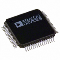
ADE7166ASTZF8 Analog Devices Inc, ADE7166ASTZF8 Datasheet - Page 17

ADE7166ASTZF8
Manufacturer Part Number
ADE7166ASTZF8
Description
IC ENERGY METER 1PHASE 64LQFP
Manufacturer
Analog Devices Inc
Specifications of ADE7166ASTZF8
Applications
Energy Measurement
Core Processor
8052
Program Memory Type
FLASH (8 kB)
Controller Series
ADE71xx
Ram Size
512 x 8
Interface
I²C, SPI, UART
Number Of I /o
20
Voltage - Supply
3.135 V ~ 3.465 V
Operating Temperature
-40°C ~ 85°C
Mounting Type
Surface Mount
Package / Case
64-LQFP
Ic Function
Single Phase Energy Measurement IC
Supply Voltage Range
3.13V To 3.46V, 2.4V To 3.7V
Operating Temperature Range
-40°C To +85°C
Digital Ic Case Style
LQFP
No. Of Pins
64
Lead Free Status / RoHS Status
Lead free / RoHS Compliant
Available stocks
Company
Part Number
Manufacturer
Quantity
Price
Company:
Part Number:
ADE7166ASTZF8
Manufacturer:
Analog Devices Inc
Quantity:
10 000
Company:
Part Number:
ADE7166ASTZF8-RL
Manufacturer:
Analog Devices Inc
Quantity:
10 000
Pin No.
43
44
45
46
47
48
49, 50
51
52, 53
54
55
56
57
58
59
60
61
62
63
64
Mnemonic
P0.2/CF1/RTCCAL
SDEN/P2.3
BCTRL/INT1/P0.0
XTAL2
XTAL1
INT0
V
EA
I
AGND
FP26 or I
RESET
REF
V
V
V
V
V
DGND
V
P
P
BAT
INTA
DD
SWOUT
INTD
DCIN
or I
, V
IN/OUT
N
PA
, I
N
PB
Description
This pin provides the ground reference for the analog circuitry.
This pin provides the ground reference for the digital circuitry.
General-Purpose Digital I/O Port 0.2, Calibration Frequency Logic Output 1, or RTC Calibration Frequency
Logic Output. The CF1 logic output gives instantaneous active, reactive, I
The RTCCAL logic output gives access to the calibrated RTC output.
Serial Download Mode Enable or Digital Output Pin P2.3. This pin is used to enable serial download mode
through a resistor when pulled low on power-up or reset. On reset, this pin momentarily becomes an input
and the status of the pin is sampled. If there is no pull-down resistor in place, the pin momentarily goes high
and then user code is executed. If the pin is pulled down on reset, the embedded serial download/debug
kernel executes, and this pin remains low during the internal program execution. After reset, this pin can be
used as a digital output port pin (P2.3).
Digital Input for Battery Control, External Interrupt Input 1, or General-Purpose Digital I/O Port 0.0. This logic
input connects V
open, the connection between V
A crystal can be connected across this pin and XTAL1 (see XTAL1 pin description) to provide a clock source
for the ADE7566/ADE7569/ADE7166/ADE7169. The XTAL2 pin can drive one CMOS load when an external
clock is supplied at XTAL1 or by the gate oscillator circuit. An internal 6 pF capacitor is connected to this pin.
An external clock can be provided at this logic input. Alternatively, a parallel resonant AT crystal can be
connected across XTAL1 and XTAL2 to provide a clock source for the ADE7566/ADE7569/ADE7166/ADE7169.
The clock frequency for specified operation is 32.768 kHz. An internal 6 pF capacitor is connected to this pin.
External Interrupt Input 0.
Analog Inputs for Voltage Channel. These inputs are fully differential voltage inputs with a maximum
differential level of ±400 mV for specified operation. This channel also has an internal PGA.
This pin is used as an input for emulation. When held high, this input enables the device to fetch code from
internal program memory locations. The ADE7566/ADE7569/ADE7166/ADE7169 do not support external
code memory. This pin should not be left floating.
Analog Inputs for Current Channel. These inputs are fully differential voltage inputs with a maximum
differential level of ±400 mV for specified operation. This channel also has an internal PGA.
LCD Segment Output 26 (FP26) for ADE7566 and ADE7569 or Analog Inputs for Second Current Channel (I
for ADE7166 and ADE7169. This input is fully differential with a maximum differential level of ±400 mV
referred to I
Reset Input, Active Low.
This pin provides access to the on-chip voltage reference. The on-chip reference has a nominal value of
1.2 V ± 0.1% and a typical temperature coefficient of 50 ppm/°C maximum. This pin should be decoupled
with a 1 μF capacitor in parallel with a ceramic 100 nF capacitor.
Power Supply Input from the Battery with a 2.4 V to 2.7 V Range. This pin is connected internally to V
the battery is selected as the power supply for the ADE7566/ADE7569/ADE7166/ADE7169.
This pin provides access to the on-chip 2.5 V analog LDO. No external active circuitry should be connected to
this pin. This pin should be decoupled with a 10 μF capacitor in parallel with a ceramic 100 nF capacitor.
3.3 V Power Supply Input from the Regulator. This pin is connected internally to V
selected as the power supply for the ADE7566/ADE7569/ADE7166/ADE7169. This pin should be decoupled
with a 10 μF capacitor in parallel with a ceramic 100 nF capacitor.
3.3 V Power Supply Output. This pin provides the supply voltage for the LDOs and internal circuitry of the
ADE7566/ADE7569/ADE7166/ADE7169. This pin should be decoupled with a 10 μF capacitor in parallel with
a ceramic 100 nF capacitor.
This pin provides access to the on-chip 2.5 V digital LDO. No external active circuitry should be connected to
this pin. This pin should be decoupled with a 10 μF capacitor in parallel with a ceramic 100 nF capacitor.
Analog Input for DC Voltage Monitoring. The maximum input voltage on this pin is V
AGND. This pin is used to monitor the preregulated dc voltage.
N
for specified operation. This channel also has an internal PGA.
DD
or V
BAT
to V
Rev. A | Page 17 of 144
SWOUT
DD
internally when set to logic high or logic low, respectively. When left
or V
BAT
and V
ADE7566/ADE7569/ADE7166/ADE7169
SWOUT
is selected internally.
rms
, or apparent power information.
DD
when the regulator is
SWOUT
with respect to
DD
when
PB
)


