ADE7166ASTZF8 Analog Devices Inc, ADE7166ASTZF8 Datasheet - Page 81

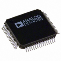
ADE7166ASTZF8
Manufacturer Part Number
ADE7166ASTZF8
Description
IC ENERGY METER 1PHASE 64LQFP
Manufacturer
Analog Devices Inc
Specifications of ADE7166ASTZF8
Applications
Energy Measurement
Core Processor
8052
Program Memory Type
FLASH (8 kB)
Controller Series
ADE71xx
Ram Size
512 x 8
Interface
I²C, SPI, UART
Number Of I /o
20
Voltage - Supply
3.135 V ~ 3.465 V
Operating Temperature
-40°C ~ 85°C
Mounting Type
Surface Mount
Package / Case
64-LQFP
Ic Function
Single Phase Energy Measurement IC
Supply Voltage Range
3.13V To 3.46V, 2.4V To 3.7V
Operating Temperature Range
-40°C To +85°C
Digital Ic Case Style
LQFP
No. Of Pins
64
Lead Free Status / RoHS Status
Lead free / RoHS Compliant
Available stocks
Company
Part Number
Manufacturer
Quantity
Price
Company:
Part Number:
ADE7166ASTZF8
Manufacturer:
Analog Devices Inc
Quantity:
10 000
Company:
Part Number:
ADE7166ASTZF8-RL
Manufacturer:
Analog Devices Inc
Quantity:
10 000
STANDARD 8052 SFRS
The standard 8052 special function registers include the
Accumulator, B, PSW, DPTR, and SP SFRs described in the
Basic 8052 Registers section. The standard 8052 SFRs also
define timers, the serial port interface, interrupts, I/O ports,
and power-down modes.
Timer SFRs
The 8052 contains three 16-bit timers: the identical Timer0 and
Timer1, as well as a Timer2. These timers can also function as
event counters. Timer2 has a capture feature where the value of
the timer can be captured in two 8-bit registers upon the
assertion of an external input signal (see
Timers section).
Serial Port SFRs
The full-duplex serial port peripheral requires two registers,
one for setting up the baud rate and other communication
parameters, and another for the transmit/receive buffer. The
ADE7566/ADE7569/ADE7166/ADE7169 also have enhanced
serial port functionality with a dedicated timer for baud rate
generation with a fractional divisor and additional error
detection. See
Interrupt SFRs
There is a two-tiered interrupt system standard in the 8052 core.
The priority level for each interrupt source is individually
selectable as high or low. The ADE7566/ADE7569/ADE7166/
ADE7169 enhance this interrupt system by creating, in essence,
a third interrupt tier for a highest priority, the power supply
management interrupt (PSM). See the
I/O Port SFRs
The 8052 core supports four I/O ports, Port 0 through Port 3,
where Port 0 and Port 2 are typically used to access external
code and data spaces. The ADE7566/ADE7569/ADE7166/
ADE7169, unlike standard 8052 products, provide internal
nonvolatile flash memory so that an external code space is
unnecessary. The on-chip LCD driver requires many pins, some
of which are dedicated for LCD functionality, and others that
can be configured as LCD or general-purpose inputs/outputs.
Due to the limited number of I/O pins, the ADE7566/ADE7569/
ADE7166/ADE7169 do not allow access to external code and
data spaces.
The ADE7566/ADE7569/ADE7166/ADE7169 provide 20 pins
that can be used for general-purpose I/O. These pins are mapped
to Port 0, Port 1, and Port 2. They are accessed through three bit-
addressable 8052 SFRs, P0, P1, and P2. Another enhanced
feature of the ADE7566/ADE7569/ADE7166/ADE7169 is that
the weak pull-ups standard on 8052 Port 1, Port 2, and Port 3
can be disabled to make open drain outputs, as is standard on
Port 0. The weak pull-ups can be enabled on a pin-by-pin basis.
See the I/O Ports section.
Table 131 and the UART Serial Interface section.
Interrupt System section.
Table 102 and the
Rev. A | Page 81 of 144
Program Control Register (PCON, 0x87)
The 8052 core defines two power-down modes: power down
and idle. The ADE7566/ADE7569/ADE7166/ADE7169
enhance the power control capability of the traditional 8052
MCU with additional power management functions. The Power
Control SFR (POWCON, 0xC5) is used to define power
control-specific functionality for the ADE7566/ADE7569/
ADE7166/ADE7169. The Program Control SFR (PCON, 0x87) is
not bit addressable. See the
The ADE7566/ADE7569/ADE7166/ADE7169 have many other
peripherals not standard to the 8052 core, including
•
•
•
•
•
•
•
•
•
MEMORY OVERVIEW
The ADE7566/ADE7569/ADE7166/ADE7169 contain the
following memory blocks:
•
•
•
The 256 bytes of general-purpose RAM share the upper 128 bytes
of its address space with special function registers. All of the
memory spaces are shown in
specifies which memory space to access.
General-Purpose RAM
General-purpose RAM resides in the 0x00 through 0xFF
memory locations. It contains the register banks.
BITS IN PSW
SELECTED
ADE7566/ADE7569/ADE7166/ADE7169
ADE energy measurement DSP
RTC
LCD driver
Battery switchover/power management
Temperature ADC
Battery ADC
SPI/I
Flash memory controller
Watchdog timer
16 kB of on-chip Flash/EE program and data memory
256 bytes of general-purpose RAM
256 bytes of internal extended RAM (XRAM)
BANKS
VIA
2
Figure 82. Lower 128 Bytes of Internal Data Memory
C communication
11
10
01
00
0x30
0x20
0x18
0x10
0x08
0x 00
Power Management section.
Figure 80. The addressing mode
0x7F
0x2F
0x1F
0x17
0x0F
0x07
FOUR BANKS OF EIGHT
REGISTERS R0 TO R7
BIT-ADDRESSABLE
(BIT ADDRESSES)
GENERAL-PURPOSE
AREA
RESET VALUE OF
STACK POINTER


