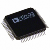
ADE7166ASTZF8 Analog Devices Inc, ADE7166ASTZF8 Datasheet - Page 80

ADE7166ASTZF8
Manufacturer Part Number
ADE7166ASTZF8
Description
IC ENERGY METER 1PHASE 64LQFP
Manufacturer
Analog Devices Inc
Specifications of ADE7166ASTZF8
Applications
Energy Measurement
Core Processor
8052
Program Memory Type
FLASH (8 kB)
Controller Series
ADE71xx
Ram Size
512 x 8
Interface
I²C, SPI, UART
Number Of I /o
20
Voltage - Supply
3.135 V ~ 3.465 V
Operating Temperature
-40°C ~ 85°C
Mounting Type
Surface Mount
Package / Case
64-LQFP
Ic Function
Single Phase Energy Measurement IC
Supply Voltage Range
3.13V To 3.46V, 2.4V To 3.7V
Operating Temperature Range
-40°C To +85°C
Digital Ic Case Style
LQFP
No. Of Pins
64
Lead Free Status / RoHS Status
Lead free / RoHS Compliant
Available stocks
Company
Part Number
Manufacturer
Quantity
Price
Company:
Part Number:
ADE7166ASTZF8
Manufacturer:
Analog Devices Inc
Quantity:
10 000
Company:
Part Number:
ADE7166ASTZF8-RL
Manufacturer:
Analog Devices Inc
Quantity:
10 000
ADE7566/ADE7569/ADE7166/ADE7169
BASIC 8052 REGISTERS
Program Counter (PC)
The program counter holds the two byte address of the next
instruction to be fetched. The PC is initialized with 0x00 at reset
and is incremented after each instruction is performed. Note
that the amount added to the PC depends on the number of
bytes in the instruction, so the increment can range from one
byte to three bytes. The program counter is not directly accessible
to the user but can be directly modified by CALL and JMP
instructions that change which part of the program is active.
Instruction Register (IR)
The instruction register holds the operations code of the
instruction being executed. The operations code is the binary
code that results from assembling an instruction. This register is
not directly accessible to the user.
Register Banks
There are four banks that each contain eight byte-wide registers
for a total of 32 bytes of registers. These registers are convenient
for temporary storage of mathematical operands. An
instruction involving the accumulator and a register can be
executed in one clock cycle, as opposed to two clock cycles to
perform an instruction involving the accumulator and a literal or
a byte of general-purpose RAM. The register banks are located in
the first 32 bytes of RAM.
The active register bank is selected by the RS0 and RS1 bits in
the Program Status Word SFR (PSW, 0xD0).
Accumulator
The accumulator is a working register, storing the results of
many arithmetic or logical operations. The accumulator is used
in more than half of the 8052 instructions where it is usually
referred to as “A. ” The program status register (PSW) constantly
monitors the number of bits that are set in the accumulator to
determine if it has even or odd parity. The accumulator is stored
in the SFR space (see Table 55).
B Register
The B register is used by the multiply and divide instructions,
MUL AB and DIV AB to hold one of the operands. Because
the B register is not used for many instructions, it can be used
as a scratch pad register such as those in the register banks.
The B register is stored in the SFR space (see Table 55).
Program Status Word (PSW)
The PSW register reflects the status of arithmetic and logical
operations through carry, auxiliary carry, and overflow flags.
The parity flag reflects the parity of the accumulator contents,
which can be helpful for communication protocols. The PSW
bits are described in
(PSW, 0xD0) is bit addressable.
Table 56. The Program Status Word SFR
Rev. A | Page 80 of 144
Data Pointer (DPTR)
The data pointer is made up of two 8-bit registers: DPH (high
byte) and DPL (low byte). These provide memory addresses for
internal code and data access. The DPTR can be manipulated as
a 16-bit register (DPTR = DPH, DPL) or as two independent
8-bit registers (DPH, DPL). See
The ADE7566/ADE7569/ADE7166/ADE7169 support dual
data pointers. See the Dual Data Pointers section. Note that the
Dual Data Pointers section of the data sheet is the only place
where the main and shadow data pointers are distinguished.
Whenever the data pointer (DPTR) is mentioned elsewhere in
the data sheet, active DPTR is implied.
Stack Pointer (SP)
The stack pointer keeps track of the current address at the top
of the stack. To push a byte of data onto the stack, the stack
pointer is incremented and the data is moved to the new top of
the stack. To pop a byte of data off the stack, the top byte of data
is moved into the awaiting address, and the stack pointer is
decremented. The stack is a last in, first out (LIFO) method of
data storage because the most recent addition to the stack is the
first to come off it.
The stack is utilized during CALL and RET instructions to keep
track of the address to move into the PC when returning from
the function call. The stack is also manipulated when vectoring
for interrupts to keep track of the prior state of the PC.
The stack resides in the internal extended RAM, and the
SP register holds the address of the stack in the extended RAM
(XRAM). The advantage of this solution is that the stack is
segregated to the internal XRAM. The use of the general-
purpose RAM can be limited to data storage, and the use of the
extended internal RAM can be limited to the stack pointer. This
separation limits the chance of data RAM corruption when the
stack pointer overflows in data RAM.
Data can still be stored in XRAM by using the MOVX command.
To change the default starting address for the stack, move a
value into the stack pointer (SP). For example, to enable the
extended stack pointer and initialize it at the beginning of the
XRAM space, use the following code:
MOV
0xFF
0x00
SP,#00H
256 BYTES OF
(DATA)
RAM
Figure 81. Extended Stack Pointer Operation
0xFF
0x00
Table 58 and Table 59.
ON-CHIP XRAM
DATA + STACK
256 BYTES OF


