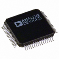
ADE7166ASTZF8 Analog Devices Inc, ADE7166ASTZF8 Datasheet - Page 33

ADE7166ASTZF8
Manufacturer Part Number
ADE7166ASTZF8
Description
IC ENERGY METER 1PHASE 64LQFP
Manufacturer
Analog Devices Inc
Specifications of ADE7166ASTZF8
Applications
Energy Measurement
Core Processor
8052
Program Memory Type
FLASH (8 kB)
Controller Series
ADE71xx
Ram Size
512 x 8
Interface
I²C, SPI, UART
Number Of I /o
20
Voltage - Supply
3.135 V ~ 3.465 V
Operating Temperature
-40°C ~ 85°C
Mounting Type
Surface Mount
Package / Case
64-LQFP
Ic Function
Single Phase Energy Measurement IC
Supply Voltage Range
3.13V To 3.46V, 2.4V To 3.7V
Operating Temperature Range
-40°C To +85°C
Digital Ic Case Style
LQFP
No. Of Pins
64
Lead Free Status / RoHS Status
Lead free / RoHS Compliant
Available stocks
Company
Part Number
Manufacturer
Quantity
Price
Company:
Part Number:
ADE7166ASTZF8
Manufacturer:
Analog Devices Inc
Quantity:
10 000
Company:
Part Number:
ADE7166ASTZF8-RL
Manufacturer:
Analog Devices Inc
Quantity:
10 000
OPERATING MODES
PSM0 (NORMAL MODE)
In PSM0, normal operating mode, V
All of the analog circuitry and digital circuitry powered by
V
default clock frequency, f
reset or software reset, is 1.024 MHz.
PSM1 (BATTERY MODE)
In PSM1, battery mode, V
operating mode, the 8052 core and all of the digital circuitry are
enabled by default. The analog circuitry for the ADE energy
metering DSP powered by V
automatically restarts, and the switch to the V
occurs when the V
PWRDN bit in the MODE1 register (0x0B) is cleared (see
Table 32). The default f
power-on reset or software reset, is 1.024 MHz.
PSM2 (SLEEP MODE)
PSM2 is a low power consumption sleep mode for use in battery
operation. In this mode, V
2.5 V digital and analog circuitry powered through V
are disabled, including the MCU core, resulting in the following:
Table 27. SFR Maintained in PSM2
I/O Configuration
Interrupt Pins Configuration SFR
(INTPR, 0xFF), see Table 16
Peripheral Configuration SFR (PERIPH,
0xF4), see Table 19
Port 0 Weak Pull-Up Enable SFR
(PINMAP0, 0xB2), see Table 150
Port 1 Weak Pull-Up Enable SFR
(PINMAP1, 0xB3), see Table 151
Port 2 Weak Pull-Up Enable SFR
(PINMAP2, 0xB4), see Table 152
Scratch Pad 1 SFR (SCRATCH1, 0xFB),
see Table 21
Scratch Pad 2 SFR (SCRATCH2, 0xFC),
see Table 22
Scratch Pad 3 SFR (SCRATCH3, 0xFD),
see Table 23
Scratch Pad 4 SFR (SCRATCH4, 0xFE),
see Table 24
INTD
and V
INTA
are enabled by default. In normal mode, the
DD
supply is above 2.75 V and when the
CORE
CORE
SWOUT
SWOUT
for PSM1, established during a
INTA
, established during a power-on
is connected to V
is connected to V
is disabled. This analog circuitry
SWOUT
Power Supply Monitoring
Battery Detection Threshold SFR
(BATVTH, 0xFA), see Table 51
Battery Switchover Configura-tion
SFR (BATPR, 0xF5), see Table 18
Battery ADC Value SFR
(BATADC, 0xDF), see Table 53
Peripheral ADC Strobe Period SFR
(STRBPER, 0xF9), see Table 48
Temperature and Supply Delta SFR
(DIFFPROG, 0xF3), see Table 49
VDCIN ADC Value SFR
(VDCINADC, 0xEF), see Table 52
Temperature ADC Value SFR
(TEMPADC, 0xD7), see Table 54
is connected to V
DD
BAT
power supply
BAT
. In this
INTA
. All of the
and V
DD
Rev. A | Page 33 of 144
INTD
.
RTC Peripherals
RTC Nominal Compensation SFR
(RTCCOMP, 0xF6), see Table 126
RTC Temperature Compensation
SFR (TEMPCAL, 0xF7), see Table 127
RTC Configuration SFR (TIMECON,
0xA1), see Table 120
Hundredths of a Second Counter
SFR (HTHSEC, 0xA2), see Table 121
Seconds Counter SFR (SEC, 0xA3),
see Table 122
Minutes Counter SFR (MIN, 0xA4),
see Table 123
Hours Counter SFR (HOUR, 0xA5),
see Table 124
Alarm Interval SFR (INTVAL, 0xA6),
see Table 125
•
•
The 3.3 V peripherals (temperature ADC, VDCIN ADC, RTC,
and LCD) are active in PSM2. They can be enabled or disabled
to reduce power consumption and are configured for PSM2
operation when the MCU core is active (see Table 28 for more
information about the individual peripherals and their PSM2
configuration). The ADE7566/ADE7569/ADE7166/ADE7169
remain in PSM2 until an event occurs to wake them up.
In PSM2, the ADE7566/ADE7569/ADE7166/ADE7169 provide
four scratch pad RAM SFRs that are maintained during this
mode. These SFRs can be used to save data from PSM0 or
PSM1 when entering PSM2 (see Table 21 to Table 24).
In PSM2, the ADE7566/ADE7569/ADE7166/ADE7169
maintain some SFRs (see Table 27). The SFRs that are not listed
in this table should be restored when the part enters PSM0 or
PSM1 from PSM2.
ADE7566/ADE7569/ADE7166/ADE7169
The RAM in the MCU is no longer valid.
The program counter for the 8052, also held in volatile
memory, becomes invalid when the 2.5 V supply is shut
down. Therefore, the program does not resume from
where it left off but always starts from the power-on reset
vector when the ADE7566/ADE7569/ADE7166/ADE7169
exit PSM2.
LCD Peripherals
LCD Segment Enable 2 SFR
(LCDSEGE2, 0xED), see Table 88
LCD Configuration Y SFR
(LCDCONY, 0xB1),see Table 81
LCD Configuration X SFR
(LCDCONX, 0x9C), see Table 79
LCD Configuration SFR
(LCDCON, 0x95), see Table 78
LCD Clock SFR (LCDCLK, 0x96),
see Table 82
LCD Segment Enable SFR
(LCDSEGE, 0x97) see Table 85
LCD Pointer SFR (LCDPTR, 0xAC),
see Table 86
LCD Data SFR (LCDDAT, 0xAE),
see Table 87


