PIC18F65K90-I/MR Microchip Technology, PIC18F65K90-I/MR Datasheet - Page 558
PIC18F65K90-I/MR
Manufacturer Part Number
PIC18F65K90-I/MR
Description
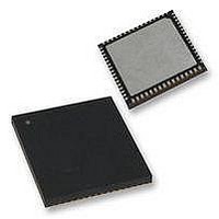
32kB Flash, 2kB RAM, 1kB EE, NanoWatt XLP, LCD 64 QFN 9x9x0.9mm TUBE
Manufacturer
Microchip Technology
Series
PIC® XLP™ 18Fr
Datasheet
1.PIC18F65K90-IMR.pdf
(570 pages)
Specifications of PIC18F65K90-I/MR
Processor Series
PIC18F
Core
PIC
Data Bus Width
8 bit
Program Memory Type
Flash
Program Memory Size
32 KB
Data Ram Size
2 KB
Interface Type
I2C, SPI
Maximum Clock Frequency
64 MHz
Number Of Timers
8
Operating Supply Voltage
1.8 V to 5.5 V
Maximum Operating Temperature
+ 125 C
3rd Party Development Tools
52715-96, 52716-328, 52717-734, 52712-325, EWPIC18
Minimum Operating Temperature
- 40 C
On-chip Adc
12 bit, 16 Channel
Core Processor
PIC
Core Size
8-Bit
Speed
64MHz
Connectivity
I²C, LIN, SPI, UART/USART
Peripherals
Brown-out Detect/Reset, LCD, POR, PWM, WDT
Number Of I /o
53
Eeprom Size
1K x 8
Ram Size
2K x 8
Voltage - Supply (vcc/vdd)
1.8 V ~ 5.5 V
Data Converters
A/D 16x12b
Oscillator Type
Internal
Operating Temperature
-40°C ~ 85°C
Package / Case
64-VFQFN Exposed Pad
Lead Free Status / Rohs Status
Details


PIC18F87K90 FAMILY
Extended Instruction Set
External Oscillator Modes
F
Fail-Safe Clock Monitor............................................. 425, 445
Fast Register Stack............................................................. 89
Firmware Instructions........................................................ 451
Flash Program Memory..................................................... 111
FSCM. See Fail-Safe Clock Monitor.
G
GOTO................................................................................ 472
H
Hardware Multiplier ........................................................... 127
High/Low-Voltage Detect .................................................. 401
DS39957D-page 558
Synchronous Slave Mode ......................................... 371
ADDFSR ................................................................... 494
ADDULNK................................................................. 494
CALLW...................................................................... 495
MOVSF ..................................................................... 495
MOVSS ..................................................................... 496
PUSHL ...................................................................... 496
SUBFSR ................................................................... 497
SUBULNK ................................................................. 497
Clock Input (EC, ECPLL Modes) ................................ 48
HS, HSPLL.................................................................. 46
Exiting Operation ...................................................... 445
Interrupts in Power-Managed Modes ........................ 446
POR or Wake from Sleep ......................................... 446
WDT During Oscillator Failure .................................. 445
Associated Registers ................................................ 119
Control Registers ...................................................... 112
Erasing ...................................................................... 116
Operation During Code-Protect ................................ 119
Protection Against Spurious Writes .......................... 119
Reading..................................................................... 115
Table Pointer
Table Pointer Boundaries ......................................... 114
Table Reads, Table Writes ....................................... 111
Writing
Writing To.................................................................. 117
8 x 8 Multiplication Algorithms .................................. 127
Operation .................................................................. 127
Performance Comparison (table) .............................. 127
Applications............................................................... 404
Associated Registers ................................................ 405
Current Consumption ................................................ 403
Effects of a Reset...................................................... 405
Operation .................................................................. 402
Associated Registers, Receive ......................... 372
Associated Registers, Transmit ........................ 371
Reception.......................................................... 372
Transmission..................................................... 371
EECON1, EECON2 .......................................... 112
TABLAT (Table Latch) ...................................... 114
TBLPTR (Table Pointer) ................................... 114
Sequence.......................................................... 116
Boundaries Based on Operation....................... 114
Unexpected Termination................................... 119
Verify................................................................. 119
Sequence.......................................................... 117
During Sleep ..................................................... 405
HLVD. See High/Low-Voltage Detect.
I
I/O Ports............................................................................ 153
I
ID Locations.............................................................. 425, 450
INCF ................................................................................. 472
INCFSZ............................................................................. 473
In-Circuit Debugger........................................................... 450
In-Circuit Serial Programming (ICSP)....................... 425, 450
Indexed Literal Offset Addressing
Indexed Literal Offset Mode.............................................. 498
Indirect Addressing ........................................................... 105
INFSNZ............................................................................. 473
Instruction Cycle ................................................................. 90
2
C Mode (MSSP)
Setup ........................................................................ 403
Start-up Time ............................................................ 403
Typical Low-Voltage Detect Application ................... 404
Open-Drain Outputs.................................................. 154
Output Pin Drive ....................................................... 153
Pin Capabilities ......................................................... 153
Pull-up Configuration ................................................ 153
Acknowledge Sequence Timing ............................... 342
Associated Registers ................................................ 348
Baud Rate Generator ............................................... 335
Bus Collision
Clock Arbitration ....................................................... 336
Clock Stretching........................................................ 328
Clock Synchronization and the CKP bit .................... 329
Effects of a Reset ..................................................... 343
General Call Address Support .................................. 332
I
Master Mode............................................................. 333
Multi-Master Communication, Bus Collision
Multi-Master Mode .................................................... 343
Operation .................................................................. 318
Read/Write Bit Information (R/W Bit) ................ 318, 321
Registers .................................................................. 313
Serial Clock (SCLx) .................................................. 321
Slave Mode............................................................... 318
Sleep Operation........................................................ 343
Stop Condition Timing .............................................. 342
and Standard PIC18 Instructions.............................. 498
Clocking Scheme........................................................ 90
Flow/Pipelining............................................................ 90
2
C Clock Rate w/BRG.............................................. 335
During a Repeated Start Condition................... 346
During a Stop Condition ................................... 347
10-Bit Slave Receive Mode (SEN = 1) ............. 328
10-Bit Slave Transmit Mode ............................. 328
7-Bit Slave Receive Mode (SEN = 1) ............... 328
7-Bit Slave Transmit Mode ............................... 328
Operation.......................................................... 334
Reception ......................................................... 339
Repeated Start Condition Timing ..................... 338
Start Condition Timing ...................................... 337
Transmission .................................................... 339
and Arbitration .................................................. 343
Address Masking Modes
Addressing........................................................ 318
Reception ......................................................... 321
Transmission .................................................... 321
5-Bit .......................................................... 319
7-Bit .......................................................... 320
2009-2011 Microchip Technology Inc.
Related parts for PIC18F65K90-I/MR
Image
Part Number
Description
Manufacturer
Datasheet
Request
R

Part Number:
Description:
Manufacturer:
Microchip Technology Inc.
Datasheet:
Part Number:
Description:
Manufacturer:
Microchip Technology Inc.
Datasheet:
Part Number:
Description:
Manufacturer:
Microchip Technology Inc.
Datasheet:
Part Number:
Description:
Manufacturer:
Microchip Technology Inc.
Datasheet:
Part Number:
Description:
Manufacturer:
Microchip Technology Inc.
Datasheet:
Part Number:
Description:
Manufacturer:
Microchip Technology Inc.
Datasheet:
Part Number:
Description:
Manufacturer:
Microchip Technology Inc.
Datasheet:
Part Number:
Description:
Manufacturer:
Microchip Technology Inc.
Datasheet: