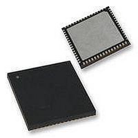
PIC18F65K90-I/MR Microchip Technology, PIC18F65K90-I/MR Datasheet - Page 398

PIC18F65K90-I/MR
Manufacturer Part Number
PIC18F65K90-I/MR
Description
32kB Flash, 2kB RAM, 1kB EE, NanoWatt XLP, LCD 64 QFN 9x9x0.9mm TUBE
Manufacturer
Microchip Technology
Series
PIC® XLP™ 18Fr
Datasheet
1.PIC18F65K90-IMR.pdf
(570 pages)
Specifications of PIC18F65K90-I/MR
Processor Series
PIC18F
Core
PIC
Data Bus Width
8 bit
Program Memory Type
Flash
Program Memory Size
32 KB
Data Ram Size
2 KB
Interface Type
I2C, SPI
Maximum Clock Frequency
64 MHz
Number Of Timers
8
Operating Supply Voltage
1.8 V to 5.5 V
Maximum Operating Temperature
+ 125 C
3rd Party Development Tools
52715-96, 52716-328, 52717-734, 52712-325, EWPIC18
Minimum Operating Temperature
- 40 C
On-chip Adc
12 bit, 16 Channel
Core Processor
PIC
Core Size
8-Bit
Speed
64MHz
Connectivity
I²C, LIN, SPI, UART/USART
Peripherals
Brown-out Detect/Reset, LCD, POR, PWM, WDT
Number Of I /o
53
Eeprom Size
1K x 8
Ram Size
2K x 8
Voltage - Supply (vcc/vdd)
1.8 V ~ 5.5 V
Data Converters
A/D 16x12b
Oscillator Type
Internal
Operating Temperature
-40°C ~ 85°C
Package / Case
64-VFQFN Exposed Pad
Lead Free Status / Rohs Status
Details
- Current page: 398 of 570
- Download datasheet (5Mb)
PIC18F87K90 FAMILY
FIGURE 25-1:
25.2
The full range of voltage reference cannot be realized
due to the construction of the module. The transistors
on the top and bottom of the resistor ladder network
(Figure
ence source rails. The voltage reference is derived
from the reference source; therefore, the CV
changes with fluctuations in that source. The tested
absolute accuracy of the voltage reference can be
found in
25.3
When the device wakes up from Sleep through an
interrupt or a Watchdog Timer time-out, the contents of
the CVRCON register are not affected. To minimize
current consumption in Sleep mode, the voltage
reference should be disabled.
DS39957D-page 398
25-1) keep CV
Section 31.0 “Electrical Characteristics”
Voltage Reference Accuracy/Error
Operation During Sleep
CVREN
V
V
AV
REF
REF
DD
REF
COMPARATOR VOLTAGE REFERENCE BLOCK DIAGRAM
+
-
from approaching the refer-
CVRSS = 1
CVRSS = 0
CVRSS = 1
CVRSS = 0
32 Steps
REF
output
.
R
R
R
R
R
R
clearing bit, CVREN (CVRCON<7>). This Reset also
disconnects the reference from the RF5 pin by clearing
25.4
A device Reset disables the voltage reference by
bit, CVROE (CVRCON<6>).
25.5
The voltage reference module operates independently
of the comparator module. The output of the reference
generator may be connected to the RF5 pin if the
CVROE bit is set. Enabling the voltage reference out-
put onto RF5, when it is configured as a digital input,
will increase current consumption. Connecting RF5 as
a digital output, with CVRSS enabled, will also increase
current consumption.
The RF5 pin can be used as a simple D/A output with
limited drive capability. Due to the limited current drive
capability, a buffer must be used on the voltage
reference output for external connections to V
Figure 25-2
Effects of a Reset
Connection Considerations
CVR<4:0>
shows an example buffering technique.
2009-2011 Microchip Technology Inc.
CV
REF
REF
.
Related parts for PIC18F65K90-I/MR
Image
Part Number
Description
Manufacturer
Datasheet
Request
R

Part Number:
Description:
Manufacturer:
Microchip Technology Inc.
Datasheet:

Part Number:
Description:
Manufacturer:
Microchip Technology Inc.
Datasheet:

Part Number:
Description:
Manufacturer:
Microchip Technology Inc.
Datasheet:

Part Number:
Description:
Manufacturer:
Microchip Technology Inc.
Datasheet:

Part Number:
Description:
Manufacturer:
Microchip Technology Inc.
Datasheet:

Part Number:
Description:
Manufacturer:
Microchip Technology Inc.
Datasheet:

Part Number:
Description:
Manufacturer:
Microchip Technology Inc.
Datasheet:

Part Number:
Description:
Manufacturer:
Microchip Technology Inc.
Datasheet:


