PIC18F65K90-I/MR Microchip Technology, PIC18F65K90-I/MR Datasheet - Page 48
PIC18F65K90-I/MR
Manufacturer Part Number
PIC18F65K90-I/MR
Description
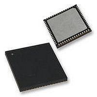
32kB Flash, 2kB RAM, 1kB EE, NanoWatt XLP, LCD 64 QFN 9x9x0.9mm TUBE
Manufacturer
Microchip Technology
Series
PIC® XLP™ 18Fr
Datasheet
1.PIC18F65K90-IMR.pdf
(570 pages)
Specifications of PIC18F65K90-I/MR
Processor Series
PIC18F
Core
PIC
Data Bus Width
8 bit
Program Memory Type
Flash
Program Memory Size
32 KB
Data Ram Size
2 KB
Interface Type
I2C, SPI
Maximum Clock Frequency
64 MHz
Number Of Timers
8
Operating Supply Voltage
1.8 V to 5.5 V
Maximum Operating Temperature
+ 125 C
3rd Party Development Tools
52715-96, 52716-328, 52717-734, 52712-325, EWPIC18
Minimum Operating Temperature
- 40 C
On-chip Adc
12 bit, 16 Channel
Core Processor
PIC
Core Size
8-Bit
Speed
64MHz
Connectivity
I²C, LIN, SPI, UART/USART
Peripherals
Brown-out Detect/Reset, LCD, POR, PWM, WDT
Number Of I /o
53
Eeprom Size
1K x 8
Ram Size
2K x 8
Voltage - Supply (vcc/vdd)
1.8 V ~ 5.5 V
Data Converters
A/D 16x12b
Oscillator Type
Internal
Operating Temperature
-40°C ~ 85°C
Package / Case
64-VFQFN Exposed Pad
Lead Free Status / Rohs Status
Details


PIC18F87K90 FAMILY
In the RC Oscillator mode, the oscillator frequency
divided by 4 is available on the OSC2 pin. This signal
may be used for test purposes or to synchronize other
logic.
connected.
FIGURE 3-3:
The RCIO Oscillator mode
the RC mode, except that the OSC2 pin becomes an
additional general purpose I/O pin. The I/O pin
becomes bit 6 of PORTA (RA6).
FIGURE 3-4:
3.5.1
The EC and ECPLL Oscillator modes require an
external clock source to be connected to the OSC1 pin.
There is no oscillator start-up time required after a
Power-on Reset or after an exit from Sleep mode.
In the EC Oscillator mode, the oscillator frequency,
divided by 4, is available on the OSC2 pin. This signal
may be used for test purposes or to synchronize other
logic.
Oscillator mode.
DS39957D-page 48
C
V
C
Recommended values: 3 k R
V
R
Recommended values: 3 k R
R
EXT
SS
EXT
SS
EXT
EXT
Figure 3-5
V
Figure 3-3
V
DD
DD
RA6
EXTERNAL CLOCK INPUT
(EC MODES)
F
OSC
shows the pin connections for the EC
shows how the R/C combination is
/4
RC OSCILLATOR MODE
OSC1
RCIO OSCILLATOR MODE
OSC1
OSC2/CLKO
I/O (OSC2)
20 pF C
20 pF C
(Figure
EXT
EXT
EXT
EXT
100 k
100 k
300 pF
3-4) functions like
300 pF
PIC18FXXXX
PIC18FXXXX
Internal
Internal
Clock
Clock
oscillating source to produce frequencies up to 64 MHz.
FIGURE 3-5:
An external clock source may also be connected to the
OSC1 pin in the HS mode, as shown in
this configuration, the divide-by-4 output on OSC2 is
not available. Current consumption in this configuration
will be somewhat higher than EC mode, as the internal
oscillator’s feedback circuitry will be enabled (in EC
mode, the feedback circuit is disabled).
FIGURE 3-6:
3.5.2
A Phase Lock Loop (PLL) circuit is provided as an
option for users who want to use a lower frequency
oscillator circuit, or to clock the device up to its highest
rated frequency from a crystal oscillator. This may be
useful for customers who are concerned with EMI due
to high-frequency crystals, or users who require higher
clock speeds from an internal oscillator.
3.5.2.1
The HSPLL and ECPLL modes provide the ability to
selectively run the device at four times the external
The PLL is enabled by setting the PLLEN bit
(OSCTUNE<6>) or the PLLCFG bit (CONFIG1H<4>).
The PLLEN bit provides software control for the PLL,
even if PLLCFG is set to ‘0’. The PLL is enabled only
when the HS or EC oscillator frequency is within the
4 MHz to 16 MHz input range.
This enables additional flexibility for controlling the
application’s clock speed in software. The PLLEN
should be enabled in HS or EC Oscillator mode only if
the input frequency is in the range of 4 MHz-16 MHz.
Clock from
Ext. System
Clock from
Ext. System
PLL FREQUENCY MULTIPLIER
F
HSPLL and ECPLL Modes
OSC
Open
/4
2009-2011 Microchip Technology Inc.
EXTERNAL CLOCK
INPUT OPERATION
(EC CONFIGURATION)
EXTERNAL CLOCK INPUT
OPERATION (HS OSC
CONFIGURATION)
OSC1/CLKI
OSC2/CLKO
OSC1
OSC2
PIC18F87K90
PIC18F87K90
(HS Mode)
Figure
3-6. In
Related parts for PIC18F65K90-I/MR
Image
Part Number
Description
Manufacturer
Datasheet
Request
R

Part Number:
Description:
Manufacturer:
Microchip Technology Inc.
Datasheet:
Part Number:
Description:
Manufacturer:
Microchip Technology Inc.
Datasheet:
Part Number:
Description:
Manufacturer:
Microchip Technology Inc.
Datasheet:
Part Number:
Description:
Manufacturer:
Microchip Technology Inc.
Datasheet:
Part Number:
Description:
Manufacturer:
Microchip Technology Inc.
Datasheet:
Part Number:
Description:
Manufacturer:
Microchip Technology Inc.
Datasheet:
Part Number:
Description:
Manufacturer:
Microchip Technology Inc.
Datasheet:
Part Number:
Description:
Manufacturer:
Microchip Technology Inc.
Datasheet: