PIC18F65K90-I/MR Microchip Technology, PIC18F65K90-I/MR Datasheet - Page 239
PIC18F65K90-I/MR
Manufacturer Part Number
PIC18F65K90-I/MR
Description
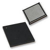
32kB Flash, 2kB RAM, 1kB EE, NanoWatt XLP, LCD 64 QFN 9x9x0.9mm TUBE
Manufacturer
Microchip Technology
Series
PIC® XLP™ 18Fr
Datasheet
1.PIC18F65K90-IMR.pdf
(570 pages)
Specifications of PIC18F65K90-I/MR
Processor Series
PIC18F
Core
PIC
Data Bus Width
8 bit
Program Memory Type
Flash
Program Memory Size
32 KB
Data Ram Size
2 KB
Interface Type
I2C, SPI
Maximum Clock Frequency
64 MHz
Number Of Timers
8
Operating Supply Voltage
1.8 V to 5.5 V
Maximum Operating Temperature
+ 125 C
3rd Party Development Tools
52715-96, 52716-328, 52717-734, 52712-325, EWPIC18
Minimum Operating Temperature
- 40 C
On-chip Adc
12 bit, 16 Channel
Core Processor
PIC
Core Size
8-Bit
Speed
64MHz
Connectivity
I²C, LIN, SPI, UART/USART
Peripherals
Brown-out Detect/Reset, LCD, POR, PWM, WDT
Number Of I /o
53
Eeprom Size
1K x 8
Ram Size
2K x 8
Voltage - Supply (vcc/vdd)
1.8 V ~ 5.5 V
Data Converters
A/D 16x12b
Oscillator Type
Internal
Operating Temperature
-40°C ~ 85°C
Package / Case
64-VFQFN Exposed Pad
Lead Free Status / Rohs Status
Details


REGISTER 18-3:
2009-2011 Microchip Technology Inc.
bit 7
Legend:
R = Readable bit
-n = Value at POR
bit 7-5
bit 4
bit 3
bit 2
bit 1-0
Note 1:
U-0
—
This bit is unimplemented and reads as ‘0’ on devices with 32 Kbytes of program memory (PIC18FX5K90).
Unimplemented: Read as ‘0’
C10TSEL0: CCP10 Timer Selection bit
0 = CCP10 is based off of TMR1/TMR2
1 = CCP10 is based off of TMR7/TMR2
Unimplemented: Read as ‘0’
C9TSEL0: CCP9 Timer Selection bit
0 = CCP9 is based off of TMR1/TMR2
1 = CCP9 is based off of TMR7/TMR4
C8TSEL<1:0>: CCP8 Timer Selection bits
On non 32-Kbyte device variants:
00 = CCP8 is based off of TMR1/TMR2
01 = CCP8 is based off of TMR7/TMR4
10 = CCP8 is based off of TMR7/TMR6
11 = Reserved; do not use
On 32-Kbyte device variants (PIC18F85K90/65K90:
00 = CCP8 is based off of TMR1/TMR2
01 = CCP8 is based off of TMR1/TMR4
10 = CCP8 is based off of TMR1/TMR6
11 = Reserved; do not use
U-0
—
CCPTMRS2: CCPx TIMER SELECT REGISTER 2
W = Writable bit
‘1’ = Bit is set
U-0
—
C10TSEL0
R/W-0
(1)
(1)
(1)
U = Unimplemented bit, read as ‘0’
‘0’ = Bit is cleared
PIC18F87K90 FAMILY
U-0
—
C9TSEL0
R/W-0
(1)
x = Bit is unknown
C8TSEL1
R/W-0
DS39957D-page 239
C8TSEL0
R/W-0
bit 0
Related parts for PIC18F65K90-I/MR
Image
Part Number
Description
Manufacturer
Datasheet
Request
R

Part Number:
Description:
Manufacturer:
Microchip Technology Inc.
Datasheet:
Part Number:
Description:
Manufacturer:
Microchip Technology Inc.
Datasheet:
Part Number:
Description:
Manufacturer:
Microchip Technology Inc.
Datasheet:
Part Number:
Description:
Manufacturer:
Microchip Technology Inc.
Datasheet:
Part Number:
Description:
Manufacturer:
Microchip Technology Inc.
Datasheet:
Part Number:
Description:
Manufacturer:
Microchip Technology Inc.
Datasheet:
Part Number:
Description:
Manufacturer:
Microchip Technology Inc.
Datasheet:
Part Number:
Description:
Manufacturer:
Microchip Technology Inc.
Datasheet: