PIC18F65K90-I/MR Microchip Technology, PIC18F65K90-I/MR Datasheet - Page 241
PIC18F65K90-I/MR
Manufacturer Part Number
PIC18F65K90-I/MR
Description
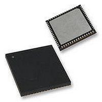
32kB Flash, 2kB RAM, 1kB EE, NanoWatt XLP, LCD 64 QFN 9x9x0.9mm TUBE
Manufacturer
Microchip Technology
Series
PIC® XLP™ 18Fr
Datasheet
1.PIC18F65K90-IMR.pdf
(570 pages)
Specifications of PIC18F65K90-I/MR
Processor Series
PIC18F
Core
PIC
Data Bus Width
8 bit
Program Memory Type
Flash
Program Memory Size
32 KB
Data Ram Size
2 KB
Interface Type
I2C, SPI
Maximum Clock Frequency
64 MHz
Number Of Timers
8
Operating Supply Voltage
1.8 V to 5.5 V
Maximum Operating Temperature
+ 125 C
3rd Party Development Tools
52715-96, 52716-328, 52717-734, 52712-325, EWPIC18
Minimum Operating Temperature
- 40 C
On-chip Adc
12 bit, 16 Channel
Core Processor
PIC
Core Size
8-Bit
Speed
64MHz
Connectivity
I²C, LIN, SPI, UART/USART
Peripherals
Brown-out Detect/Reset, LCD, POR, PWM, WDT
Number Of I /o
53
Eeprom Size
1K x 8
Ram Size
2K x 8
Voltage - Supply (vcc/vdd)
1.8 V ~ 5.5 V
Data Converters
A/D 16x12b
Oscillator Type
Internal
Operating Temperature
-40°C ~ 85°C
Package / Case
64-VFQFN Exposed Pad
Lead Free Status / Rohs Status
Details


18.1
Each Capture/Compare/PWM module is associated
with a control register (generically, CCPxCON) and a
data register (CCPRx). The data register, in turn, is
comprised of two 8-bit registers: CCPRxL (low byte)
and CCPRxH (high byte). All registers are both
readable and writable.
18.1.1
The CCP modules utilize Timers, 1 through 8, which
varies with the selected mode. Various timers are avail-
able to the CCP modules in Capture, Compare or PWM
modes, as shown in
TABLE 18-2:
TABLE 18-3:
2009-2011 Microchip Technology Inc.
C4TSEL
Note 1:
C8TSEL
Note 1:
<1:0>
<1:0>
0 0
0 1
1 0
1 1
0 0
0 1
1 0
1 1
2:
CCP Module Configuration
Compare
Compare
Capture/
Capture/
Do not use the reserved bits.
The module is not available for devices with 32 Kbytes of program memory.
Do not use the reserved bits.
CCP8
CCP4
TMR1
TMR3
TMR3
CCP MODULES AND TIMER
RESOURCES
TMR1
TMR7
TMR7
Mode
Mode
Reserved
Reserved
TIMER ASSIGNMENTS FOR CCP MODULES 4, 5, 6 AND 7
TIMER ASSIGNMENTS FOR CCP MODULES 8, 9 AND 10
Table
TMR2
TMR4
TMR6
TMR2
TMR4
TMR6
Mode
Mode
PWM
PWM
(1)
(2)
18-1.
Devices with 32 Kbytes
C8TSEL
C5TSEL0
<1:0>
0 0
0 1
1 0
1 1
0
1
Compare
Capture/
CCP8
Compare
Capture/
TMR1
TMR1
TMR1
CCP5
Mode
Reserved
TMR1
TMR5
Mode
CCPTMRS2 Register
CCPTMRS1 Register
TMR2
TMR4
TMR6
Mode
PWM
(2)
TMR2
TMR4
Mode
PWM
(1)
C9TSEL0
C6TSEL0
PIC18F87K90 FAMILY
0
1
TABLE 18-1:
The assignment of a particular timer to a module is
determined by the Timer to CCP enable bits in the
CCPTMRSx
Register
once and may share the same timer resource if they
are configured to operate in the same mode
(Capture/Compare or PWM) at the same time.
The CCPTMRS1 register selects the timers for CCP
modules, 7, 6, 5 and 4, and the CCPTMRS2 register
selects the timers for CCP modules, 10, 9 and 8. The
possible configurations are shown in
Table
0
1
CCP Mode
Compare
Capture
CCP9
PWM
Compare
Capture/
18-3.
TMR1
TMR7
Compare
Mode
Capture/
CCP6
TMR1
TMR5
18-3). All of the modules may be active at
Mode
(1)
registers
TMR2
TMR4
Mode
PWM
Timer1, Timer3, Timer 5 or Timer7
Timer2, Timer4, Timer 6 or Timer8
CCP MODE – TIMER
RESOURCE
TMR2
TMR2
Mode
PWM
C10TSEL0
Timer Resource
C7TSEL
(see
<1:0>
0
1
0 0
0 1
1 0
1 1
Register 18-2
CCP10
DS39957D-page 241
Compare
Capture/
Compare
Capture/
CCP7
TMR1
TMR7
TMR1
TMR5
TMR5
TMR5
Mode
Mode
Table 18-2
(1)
TMR2
TMR2
Mode
PWM
TMR2
TMR4
TMR6
TMR8
Mode
PWM
and
and
Related parts for PIC18F65K90-I/MR
Image
Part Number
Description
Manufacturer
Datasheet
Request
R

Part Number:
Description:
Manufacturer:
Microchip Technology Inc.
Datasheet:
Part Number:
Description:
Manufacturer:
Microchip Technology Inc.
Datasheet:
Part Number:
Description:
Manufacturer:
Microchip Technology Inc.
Datasheet:
Part Number:
Description:
Manufacturer:
Microchip Technology Inc.
Datasheet:
Part Number:
Description:
Manufacturer:
Microchip Technology Inc.
Datasheet:
Part Number:
Description:
Manufacturer:
Microchip Technology Inc.
Datasheet:
Part Number:
Description:
Manufacturer:
Microchip Technology Inc.
Datasheet:
Part Number:
Description:
Manufacturer:
Microchip Technology Inc.
Datasheet: