PIC18F65K90-I/MR Microchip Technology, PIC18F65K90-I/MR Datasheet - Page 196
PIC18F65K90-I/MR
Manufacturer Part Number
PIC18F65K90-I/MR
Description
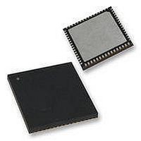
32kB Flash, 2kB RAM, 1kB EE, NanoWatt XLP, LCD 64 QFN 9x9x0.9mm TUBE
Manufacturer
Microchip Technology
Series
PIC® XLP™ 18Fr
Datasheet
1.PIC18F65K90-IMR.pdf
(570 pages)
Specifications of PIC18F65K90-I/MR
Processor Series
PIC18F
Core
PIC
Data Bus Width
8 bit
Program Memory Type
Flash
Program Memory Size
32 KB
Data Ram Size
2 KB
Interface Type
I2C, SPI
Maximum Clock Frequency
64 MHz
Number Of Timers
8
Operating Supply Voltage
1.8 V to 5.5 V
Maximum Operating Temperature
+ 125 C
3rd Party Development Tools
52715-96, 52716-328, 52717-734, 52712-325, EWPIC18
Minimum Operating Temperature
- 40 C
On-chip Adc
12 bit, 16 Channel
Core Processor
PIC
Core Size
8-Bit
Speed
64MHz
Connectivity
I²C, LIN, SPI, UART/USART
Peripherals
Brown-out Detect/Reset, LCD, POR, PWM, WDT
Number Of I /o
53
Eeprom Size
1K x 8
Ram Size
2K x 8
Voltage - Supply (vcc/vdd)
1.8 V ~ 5.5 V
Data Converters
A/D 16x12b
Oscillator Type
Internal
Operating Temperature
-40°C ~ 85°C
Package / Case
64-VFQFN Exposed Pad
Lead Free Status / Rohs Status
Details


PIC18F87K90 FAMILY
13.8.4
When Timer1 Gate Single Pulse mode is enabled, it is
possible to capture a single pulse gate event. Timer1
Gate Single Pulse mode is enabled by setting the
T1GSPM bit (T1GCON<4>) and the T1GGO/T1DONE
bit (T1GCON<3>). The Timer1 will be fully enabled on
the next incrementing edge.
On the next trailing edge of the pulse, the T1GGO/
T1DONE bit will automatically be cleared. No other
gate events will be allowed to increment Timer1 until
the T1GGO/T1DONE bit is once again set in software.
FIGURE 13-6:
DS39957D-page 196
TMR1GE
T1GSPM
T1DONE
T1GPOL
T1GGO/
T1GVAL
RTCCIF
T1G_IN
Timer1
T1CKI
TIMER1 GATE SINGLE PULSE
MODE
TIMER1 GATE SINGLE PULSE MODE
Cleared by Software
N
Counting Enabled on
Rising Edge of T1G
Set by Software
N + 1
Clearing the T1GSPM bit of the T1GCON register will
also clear the T1GGO/T1DONE bit. (For timing details,
see
Simultaneously enabling the Toggle and Single Pulse
modes will permit both sections to work together. This
allows the cycle times on the Timer1 gate source to be
measured. (For timing details, see
13.8.5
When the Timer1 gate value status is utilized, it is
possible to read the most current level of the gate
control value. The value is stored in the T1GVAL bit
(T1GCON<2>). This bit is valid even when the Timer1
gate is not enabled (TMR1GE bit is cleared).
Figure
Set by Hardware on
Falling Edge of T1GVAL
Cleared by Hardware on
Falling Edge of T1GVAL
13-6.)
TIMER1 GATE VALUE STATUS
N + 2
2009-2011 Microchip Technology Inc.
Figure
Cleared by
Software
13-7.)
Related parts for PIC18F65K90-I/MR
Image
Part Number
Description
Manufacturer
Datasheet
Request
R

Part Number:
Description:
Manufacturer:
Microchip Technology Inc.
Datasheet:
Part Number:
Description:
Manufacturer:
Microchip Technology Inc.
Datasheet:
Part Number:
Description:
Manufacturer:
Microchip Technology Inc.
Datasheet:
Part Number:
Description:
Manufacturer:
Microchip Technology Inc.
Datasheet:
Part Number:
Description:
Manufacturer:
Microchip Technology Inc.
Datasheet:
Part Number:
Description:
Manufacturer:
Microchip Technology Inc.
Datasheet:
Part Number:
Description:
Manufacturer:
Microchip Technology Inc.
Datasheet:
Part Number:
Description:
Manufacturer:
Microchip Technology Inc.
Datasheet: