PIC18F65K90-I/MR Microchip Technology, PIC18F65K90-I/MR Datasheet - Page 457
PIC18F65K90-I/MR
Manufacturer Part Number
PIC18F65K90-I/MR
Description
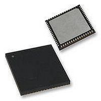
32kB Flash, 2kB RAM, 1kB EE, NanoWatt XLP, LCD 64 QFN 9x9x0.9mm TUBE
Manufacturer
Microchip Technology
Series
PIC® XLP™ 18Fr
Datasheet
1.PIC18F65K90-IMR.pdf
(570 pages)
Specifications of PIC18F65K90-I/MR
Processor Series
PIC18F
Core
PIC
Data Bus Width
8 bit
Program Memory Type
Flash
Program Memory Size
32 KB
Data Ram Size
2 KB
Interface Type
I2C, SPI
Maximum Clock Frequency
64 MHz
Number Of Timers
8
Operating Supply Voltage
1.8 V to 5.5 V
Maximum Operating Temperature
+ 125 C
3rd Party Development Tools
52715-96, 52716-328, 52717-734, 52712-325, EWPIC18
Minimum Operating Temperature
- 40 C
On-chip Adc
12 bit, 16 Channel
Core Processor
PIC
Core Size
8-Bit
Speed
64MHz
Connectivity
I²C, LIN, SPI, UART/USART
Peripherals
Brown-out Detect/Reset, LCD, POR, PWM, WDT
Number Of I /o
53
Eeprom Size
1K x 8
Ram Size
2K x 8
Voltage - Supply (vcc/vdd)
1.8 V ~ 5.5 V
Data Converters
A/D 16x12b
Oscillator Type
Internal
Operating Temperature
-40°C ~ 85°C
Package / Case
64-VFQFN Exposed Pad
Lead Free Status / Rohs Status
Details


29.1.1
ADDLW
Syntax:
Operands:
Operation:
Status Affected:
Encoding:
Description:
Words:
Cycles:
Example:
2009-2011 Microchip Technology Inc.
Q Cycle Activity:
Note:
Before Instruction
After Instruction
Decode
W
W
Q1
symbolic addressing. If a label is used, the instruction format then becomes: {label} instruction argument(s).
STANDARD INSTRUCTION SET
All PIC18 instructions may take an optional label argument preceding the instruction mnemonic for use in
=
=
10h
25h
literal ‘k’
ADD Literal to W
ADDLW
0 k 255
(W) + k W
N, OV, C, DC, Z
The contents of W are added to the
8-bit literal ‘k’ and the result is placed in
W.
1
1
ADDLW
Read
0000
Q2
15h
k
1111
Process
Data
Q3
kkkk
Write to
Q4
W
kkkk
PIC18F87K90 FAMILY
ADDWF
Syntax:
Operands:
Operation:
Status Affected:
Encoding:
Description:
Words:
Cycles:
Example:
Q Cycle Activity:
Before Instruction
After Instruction
Decode
W
REG
W
REG
Q1
=
=
=
=
register ‘f’
ADD W to f
ADDWF
0 f 255
d [ 0,1 ]
a [ 0,1 ]
(W) + (f) dest
N, OV, C, DC, Z
Add W to register ‘f’. If ‘d’ is ‘ 0 ’, the
result is stored in W. If ‘d’ is ‘ 1 ’, the
result is stored back in register ‘f’.
If ‘a’ is ‘ 0 ’, the Access Bank is selected.
If ‘a’ is ‘ 1 ’, the BSR is used to select the
GPR bank.
If ‘a’ is ‘ 0 ’ and the extended instruction
set is enabled, this instruction operates
in Indexed Literal Offset Addressing
mode whenever f 95 (5Fh). See
Section 29.2.3 “Byte-Oriented and
Bit-Oriented Instructions in Indexed
Literal Offset Mode”
1
1
ADDWF
Read
0010
Q2
17h
0C2h
0D9h
0C2h
f {,d {,a}}
01da
REG, 0, 0
Process
Data
Q3
DS39957D-page 457
ffff
for details.
destination
Write to
Q4
ffff
Related parts for PIC18F65K90-I/MR
Image
Part Number
Description
Manufacturer
Datasheet
Request
R

Part Number:
Description:
Manufacturer:
Microchip Technology Inc.
Datasheet:
Part Number:
Description:
Manufacturer:
Microchip Technology Inc.
Datasheet:
Part Number:
Description:
Manufacturer:
Microchip Technology Inc.
Datasheet:
Part Number:
Description:
Manufacturer:
Microchip Technology Inc.
Datasheet:
Part Number:
Description:
Manufacturer:
Microchip Technology Inc.
Datasheet:
Part Number:
Description:
Manufacturer:
Microchip Technology Inc.
Datasheet:
Part Number:
Description:
Manufacturer:
Microchip Technology Inc.
Datasheet:
Part Number:
Description:
Manufacturer:
Microchip Technology Inc.
Datasheet: