PIC18F65K90-I/MR Microchip Technology, PIC18F65K90-I/MR Datasheet - Page 307
PIC18F65K90-I/MR
Manufacturer Part Number
PIC18F65K90-I/MR
Description
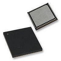
32kB Flash, 2kB RAM, 1kB EE, NanoWatt XLP, LCD 64 QFN 9x9x0.9mm TUBE
Manufacturer
Microchip Technology
Series
PIC® XLP™ 18Fr
Datasheet
1.PIC18F65K90-IMR.pdf
(570 pages)
Specifications of PIC18F65K90-I/MR
Processor Series
PIC18F
Core
PIC
Data Bus Width
8 bit
Program Memory Type
Flash
Program Memory Size
32 KB
Data Ram Size
2 KB
Interface Type
I2C, SPI
Maximum Clock Frequency
64 MHz
Number Of Timers
8
Operating Supply Voltage
1.8 V to 5.5 V
Maximum Operating Temperature
+ 125 C
3rd Party Development Tools
52715-96, 52716-328, 52717-734, 52712-325, EWPIC18
Minimum Operating Temperature
- 40 C
On-chip Adc
12 bit, 16 Channel
Core Processor
PIC
Core Size
8-Bit
Speed
64MHz
Connectivity
I²C, LIN, SPI, UART/USART
Peripherals
Brown-out Detect/Reset, LCD, POR, PWM, WDT
Number Of I /o
53
Eeprom Size
1K x 8
Ram Size
2K x 8
Voltage - Supply (vcc/vdd)
1.8 V ~ 5.5 V
Data Converters
A/D 16x12b
Oscillator Type
Internal
Operating Temperature
-40°C ~ 85°C
Package / Case
64-VFQFN Exposed Pad
Lead Free Status / Rohs Status
Details


21.3.4
To enable the serial port, MSSP Enable bit, SSPEN
(SSPxCON1<5>), must be set. To reset or reconfigure
SPI mode, clear the SSPEN bit, reinitialize the
SSPxCON registers and then set the SSPEN bit. This
configures the SDIx, SDOx, SCKx and SSx pins as
serial port pins. For the pins to behave as the serial port
function, some must have their data direction bits (in
the TRIS register) appropriately programmed as
follows:
• SDIx must have TRISC<4> or TRISD<5> bit set
• SDOx must have the TRISC<5> or TRISD<4> bit
• SCKx (Master mode) must have the TRISC<3> or
• SCKx (Slave mode) must have the TRISC<3> or
• SSx must have the TRISF<7> or TRISD<7> bit set
FIGURE 21-2:
2009-2011 Microchip Technology Inc.
cleared
TRISD<6>bit cleared
TRISD<6> bit set
ENABLING SPI I/O
SPI Master SSPM<3:0> = 00xxb
MSb
PROCESSOR 1
Serial Input Buffer
SPI MASTER/SLAVE CONNECTION
Shift Register
(SSPxBUF)
(SSPxSR)
LSb
SDOx
SCKx
SDIx
Serial Clock
PIC18F87K90 FAMILY
Any serial port function that is not desired may be
overridden by programming the corresponding Data
Direction (TRIS) register to the opposite value.
21.3.5
Figure 21-2
microcontrollers. The master controller (Processor 1)
initiates the data transfer by sending the SCKx signal.
Data is shifted out of both shift registers on their pro-
grammed clock edge and latched on the opposite edge
of the clock. Both processors should be programmed to
the same Clock Polarity (CKP), then both controllers
would send and receive data at the same time.
Whether the data is meaningful (or dummy data)
depends on the application software. This leads to
three scenarios for data transmission:
• Master sends data–Slave sends dummy data
• Master sends data–Slave sends data
• Master sends dummy data–Slave sends data
SDOx
SCKx
SDIx
TYPICAL CONNECTION
shows a typical connection between two
SPI Slave SSPM<3:0> = 010xb
MSb
Serial Input Buffer
Shift Register
(SSPxBUF)
PROCESSOR 2
(SSPxSR)
LSb
DS39957D-page 307
Related parts for PIC18F65K90-I/MR
Image
Part Number
Description
Manufacturer
Datasheet
Request
R

Part Number:
Description:
Manufacturer:
Microchip Technology Inc.
Datasheet:
Part Number:
Description:
Manufacturer:
Microchip Technology Inc.
Datasheet:
Part Number:
Description:
Manufacturer:
Microchip Technology Inc.
Datasheet:
Part Number:
Description:
Manufacturer:
Microchip Technology Inc.
Datasheet:
Part Number:
Description:
Manufacturer:
Microchip Technology Inc.
Datasheet:
Part Number:
Description:
Manufacturer:
Microchip Technology Inc.
Datasheet:
Part Number:
Description:
Manufacturer:
Microchip Technology Inc.
Datasheet:
Part Number:
Description:
Manufacturer:
Microchip Technology Inc.
Datasheet: