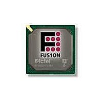
AFS250-FGG256 Actel, AFS250-FGG256 Datasheet - Page 7

AFS250-FGG256
Manufacturer Part Number
AFS250-FGG256
Description
FPGA - Field Programmable Gate Array 250K System Gates
Manufacturer
Actel
Datasheet
1.AFS600-PQG208.pdf
(330 pages)
Specifications of AFS250-FGG256
Processor Series
AFS250
Core
IP Core
Maximum Operating Frequency
1098.9 MHz
Number Of Programmable I/os
114
Data Ram Size
36864
Supply Voltage (max)
1.575 V
Maximum Operating Temperature
+ 70 C
Minimum Operating Temperature
0 C
Development Tools By Supplier
AFS-Eval-Kit, AFS-BRD600, FlashPro 3, FlashPro Lite, Silicon-Explorer II, Silicon-Sculptor 3, SI-EX-TCA
Mounting Style
SMD/SMT
Supply Voltage (min)
1.425 V
Number Of Gates
250 K
Package / Case
FPBGA-256
Lead Free Status / RoHS Status
Lead free / RoHS Compliant
Available stocks
Company
Part Number
Manufacturer
Quantity
Price
Company:
Part Number:
AFS250-FGG256
Manufacturer:
Actel
Quantity:
135
Company:
Part Number:
AFS250-FGG256
Manufacturer:
ACTEL
Quantity:
6 800
Company:
Part Number:
AFS250-FGG256I
Manufacturer:
Microsemi SoC
Quantity:
10 000
- Current page: 7 of 330
- Download datasheet (13Mb)
1 – Fusion Device Family Overview
Introduction
General Description
The Actel Fusion
simplifies design and unleashes their creativity. As the world’s first mixed signal programmable logic
family, Fusion integrates mixed signal analog, flash memory, and FPGA fabric in a monolithic device.
Actel Fusion devices enable designers to quickly move from concept to completed design and then
deliver feature-rich systems to market. This new technology takes advantage of the unique properties of
Actel flash-based FPGAs, including a high-isolation, triple-well process and the ability to support high-
voltage transistors to meet the demanding requirements of mixed signal system design.
Actel Fusion mixed signal FPGAs bring the benefits of programmable logic to many application areas,
including power management, smart battery charging, clock generation and management, and motor
control. Until now, these applications have only been implemented with costly and space-consuming
discrete analog components or mixed signal ASIC solutions. Actel Fusion mixed signal FPGAs present
new capabilities for system development by allowing designers to integrate a wide range of functionality
into a single device, while at the same time offering the flexibility of upgrades late in the manufacturing
process or after the device is in the field. Actel Fusion devices provide an excellent alternative to costly
and time-consuming mixed signal ASIC designs. In addition, when used in conjunction with the Actel
Cortex-M1, Actel Fusion technology represents the definitive mixed signal FPGA platform.
Flash-based Fusion devices are live at power-up. As soon as system power is applied and within normal
operating specifications, Fusion devices are working. Fusion devices have a 128-bit flash-based lock and
industry-leading AES decryption, used to secure programmed intellectual property (IP) and configuration
data. Actel Fusion devices are the most comprehensive single-chip analog and digital programmable
logic solution available today.
To support this new ground-breaking technology, Actel has developed a series of major tool innovations
to help maximize designer productivity. Implemented as extensions to the popular Actel Libero
Integrated Design Environment (IDE), these new tools allow designers to easily instantiate and configure
peripherals within a design, establish links between peripherals, create or import building blocks or
reference designs, and perform hardware verification. This tool suite will also add comprehensive
hardware/software debug capability as well as a suite of utilities to simplify development of embedded
soft-processor-based solutions.
The Actel Fusion family, based on the highly successful ProASIC
architecture, has been designed as a high-performance, programmable, mixed signal platform. By
combining an advanced flash FPGA core with flash memory blocks and analog peripherals, Fusion
devices dramatically simplify system design and, as a result, dramatically reduce overall system cost and
board space.
The state-of-the-art flash memory technology offers high-density integrated flash memory blocks,
enabling savings in cost, power, and board area relative to external flash solutions, while providing
increased flexibility and performance. The flash memory blocks and integrated analog peripherals enable
true mixed-mode programmable logic designs. Two examples are using an on-chip soft processor to
implement a fully functional flash MCU and using high-speed FPGA logic to offer system and power
supervisory capabilities. Live at power-up and capable of operating from a single 3.3 V supply, the Fusion
family is ideally suited for system management and control applications.
The devices in the Fusion family are categorized by FPGA core density. Each family member contains
many peripherals, including flash memory blocks, an analog-to-digital-converter (ADC), high-drive
outputs, both RC and crystal oscillators, and a real-time counter (RTC). This provides the user with a
high level of flexibility and integration to support a wide variety of mixed signal applications. The flash
memory block capacity ranges from 2 Mbits to 8 Mbits. The integrated 12-bit ADC supports up to 30
independently configurable input channels. The on-chip crystal and RC oscillators work in conjunction
®
mixed signal FPGA satisfies the demand from system architects for a device that
R e v i s i o n 1
®
3 and ProASIC3E flash FPGA
1 -1
®
Related parts for AFS250-FGG256
Image
Part Number
Description
Manufacturer
Datasheet
Request
R

Part Number:
Description:
FPGA 256/I�/Fusion Voltage: 1.5, 1.8, 2.5, 3.3 Mixed Voltage
Manufacturer:
Actel
Datasheet:

Part Number:
Description:
FPGA - Field Programmable Gate Array 250K System Gates
Manufacturer:
Actel
Datasheet:

Part Number:
Description:
MCU, MPU & DSP Development Tools Silicon Sculptor Programming Mod
Manufacturer:
Actel

Part Number:
Description:
MCU, MPU & DSP Development Tools InSystem Programming ProASICPLUS Devices
Manufacturer:
Actel

Part Number:
Description:
Programming Socket Adapters & Emulators PQ160 Module
Manufacturer:
Actel

Part Number:
Description:
Programming Socket Adapters & Emulators Axcelerator Adap Module Kit
Manufacturer:
Actel

Part Number:
Description:
Programming Socket Adapters & Emulators Evaluation
Manufacturer:
Actel

Part Number:
Description:
Programming Socket Adapters & Emulators AFDX Solutions
Manufacturer:
Actel

Part Number:
Description:
Programming Socket Adapters & Emulators SILICON SCULPTOR ADAPTER MODULE
Manufacturer:
Actel
Datasheet:

Part Number:
Description:
Programming Socket Adapters & Emulators Axcelerator Adap Module Kit
Manufacturer:
Actel

Part Number:
Description:
Programming Socket Adapters & Emulators Evaluation
Manufacturer:
Actel

Part Number:
Description:
Programming Socket Adapters & Emulators Silicon Sculptor Software
Manufacturer:
Actel

Part Number:
Description:
Programming Socket Adapters & Emulators InSystem Programming ProASICPLUS Devices
Manufacturer:
Actel


