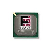
AFS250-FGG256 Actel, AFS250-FGG256 Datasheet - Page 162

AFS250-FGG256
Manufacturer Part Number
AFS250-FGG256
Description
FPGA - Field Programmable Gate Array 250K System Gates
Manufacturer
Actel
Datasheet
1.AFS600-PQG208.pdf
(330 pages)
Specifications of AFS250-FGG256
Processor Series
AFS250
Core
IP Core
Maximum Operating Frequency
1098.9 MHz
Number Of Programmable I/os
114
Data Ram Size
36864
Supply Voltage (max)
1.575 V
Maximum Operating Temperature
+ 70 C
Minimum Operating Temperature
0 C
Development Tools By Supplier
AFS-Eval-Kit, AFS-BRD600, FlashPro 3, FlashPro Lite, Silicon-Explorer II, Silicon-Sculptor 3, SI-EX-TCA
Mounting Style
SMD/SMT
Supply Voltage (min)
1.425 V
Number Of Gates
250 K
Package / Case
FPBGA-256
Lead Free Status / RoHS Status
Lead free / RoHS Compliant
Available stocks
Company
Part Number
Manufacturer
Quantity
Price
Company:
Part Number:
AFS250-FGG256
Manufacturer:
Actel
Quantity:
135
Company:
Part Number:
AFS250-FGG256
Manufacturer:
ACTEL
Quantity:
6 800
Company:
Part Number:
AFS250-FGG256I
Manufacturer:
Microsemi SoC
Quantity:
10 000
- Current page: 162 of 330
- Download datasheet (13Mb)
Device Architecture
2- 14 6
5 V Input Tolerance
I/Os can support 5 V input tolerance when LVTTL 3.3 V, LVCMOS 3.3 V, LVCMOS 2.5 V / 5 V, and
LVCMOS 2.5 V configurations are used (see
recommended solutions (see
setups) to achieve 5 V receiver tolerance. All the solutions meet a common requirement of limiting the
voltage at the input to 3.6 V or less. In fact, the I/O absolute maximum voltage rating is 3.6 V, and any
voltage above 3.6 V may cause long-term gate oxide failures.
Solution 1
The board-level design needs to ensure that the reflected waveform at the pad does not exceed the limits
provided in
This scheme will also work for a 3.3 V PCI / PCI-X configuration, but the internal diode should not be
used for clamping, and the voltage must be limited by the two external resistors, as explained below.
Relying on the diode clamping would create an excessive pad DC voltage of 3.3 V + 0.7 V = 4 V.
The following are some examples of possible resistor values (based on a simplified simulation model
with no line effects and 10 Ω transmitter output resistance, where Rtx_out_high = (V
Rtx_out_low = V
Example 1 (high speed, high current):
Rtx_out_high = Rtx_out_low = 10 Ω
Example 2 (low–medium speed, medium current):
Other values of resistors are also allowed as long as the resistors are sized appropriately to limit the
voltage at the receiving end to 2.5 V < Vin(rx) < 3.6 V when the transmitter sends a logic 1. This range of
Vin_dc(rx) must be assured for any combination of transmitter supply (5 V ± 0.5 V), transmitter output
resistance, and board resistor tolerances.
R1 = 36 Ω (±5%), P(r1)min = 0.069 Ω
R2 = 82 Ω (±5%), P(r2)min = 0.158 Ω
Imax_tx = 5.5 V / (82 * 0.95 + 36 * 0.95 + 10) = 45.04 mA
t
t
Rtx_out_high = Rtx_out_low = 10 Ω
R1 = 220 Ω (±5%), P(r1)min = 0.018 Ω
R2 = 390 Ω (±5%), P(r2)min = 0.032 Ω
Imax_tx = 5.5 V / (220 * 0.95 + 390 * 0.95 + 10) = 9.17 mA
t
t
RISE
RISE
RISE
RISE
= t
= t
= t
= t
Table 3-4 on page
FALL
FALL
FALL
FALL
OL
= 0.85 ns at C_pad_load = 10 pF (includes up to 25% safety margin)
= 4 ns at C_pad_load = 50 pF (includes up to 25% safety margin)
= 4 ns at C_pad_load = 10 pF (includes up to 25% safety margin)
= 20 ns at C_pad_load = 50 pF (includes up to 25% safety margin)
/ I
OL
).
Figure 2-101
3-4. This is a long-term reliability requirement.
to
R e visio n 1
Table 2-74 on page 2-149
Figure 2-104 on page 2-148
for more details). There are four
for details of board and macro
CCI
– V
OH
) / I
OH
,
Related parts for AFS250-FGG256
Image
Part Number
Description
Manufacturer
Datasheet
Request
R

Part Number:
Description:
FPGA 256/I�/Fusion Voltage: 1.5, 1.8, 2.5, 3.3 Mixed Voltage
Manufacturer:
Actel
Datasheet:

Part Number:
Description:
FPGA - Field Programmable Gate Array 250K System Gates
Manufacturer:
Actel
Datasheet:

Part Number:
Description:
MCU, MPU & DSP Development Tools Silicon Sculptor Programming Mod
Manufacturer:
Actel

Part Number:
Description:
MCU, MPU & DSP Development Tools InSystem Programming ProASICPLUS Devices
Manufacturer:
Actel

Part Number:
Description:
Programming Socket Adapters & Emulators PQ160 Module
Manufacturer:
Actel

Part Number:
Description:
Programming Socket Adapters & Emulators Axcelerator Adap Module Kit
Manufacturer:
Actel

Part Number:
Description:
Programming Socket Adapters & Emulators Evaluation
Manufacturer:
Actel

Part Number:
Description:
Programming Socket Adapters & Emulators AFDX Solutions
Manufacturer:
Actel

Part Number:
Description:
Programming Socket Adapters & Emulators SILICON SCULPTOR ADAPTER MODULE
Manufacturer:
Actel
Datasheet:

Part Number:
Description:
Programming Socket Adapters & Emulators Axcelerator Adap Module Kit
Manufacturer:
Actel

Part Number:
Description:
Programming Socket Adapters & Emulators Evaluation
Manufacturer:
Actel

Part Number:
Description:
Programming Socket Adapters & Emulators Silicon Sculptor Software
Manufacturer:
Actel

Part Number:
Description:
Programming Socket Adapters & Emulators InSystem Programming ProASICPLUS Devices
Manufacturer:
Actel


