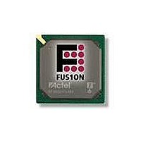
AFS250-FGG256 Actel, AFS250-FGG256 Datasheet - Page 256

AFS250-FGG256
Manufacturer Part Number
AFS250-FGG256
Description
FPGA - Field Programmable Gate Array 250K System Gates
Manufacturer
Actel
Datasheet
1.AFS600-PQG208.pdf
(330 pages)
Specifications of AFS250-FGG256
Processor Series
AFS250
Core
IP Core
Maximum Operating Frequency
1098.9 MHz
Number Of Programmable I/os
114
Data Ram Size
36864
Supply Voltage (max)
1.575 V
Maximum Operating Temperature
+ 70 C
Minimum Operating Temperature
0 C
Development Tools By Supplier
AFS-Eval-Kit, AFS-BRD600, FlashPro 3, FlashPro Lite, Silicon-Explorer II, Silicon-Sculptor 3, SI-EX-TCA
Mounting Style
SMD/SMT
Supply Voltage (min)
1.425 V
Number Of Gates
250 K
Package / Case
FPBGA-256
Lead Free Status / RoHS Status
Lead free / RoHS Compliant
Available stocks
Company
Part Number
Manufacturer
Quantity
Price
Company:
Part Number:
AFS250-FGG256
Manufacturer:
Actel
Quantity:
135
Company:
Part Number:
AFS250-FGG256
Manufacturer:
ACTEL
Quantity:
6 800
Company:
Part Number:
AFS250-FGG256I
Manufacturer:
Microsemi SoC
Quantity:
10 000
- Current page: 256 of 330
- Download datasheet (13Mb)
DC and Power Characteristics
Figure 3-1 • I/O State as a Function of VCCI and VCC Voltage Levels
3 - 6
Deactivation trip point:
V a = 0.85 V ± 0.25 V
V d = 0.75 V ± 0.25 V
Activation trip point:
VCC = 1.575 V
VCC = 1.425 V
VCC
Deactivation trip point:
Region 1: I/O Buffers are OFF
Activation trip point:
VCC = VCCI + VT
Where VT can be from 0.58 V to 0.9 V (typically 0.75 V)
V d = 0.8 V ± 0.3 V
V a = 0.9 V ±0.3 V
Region 1: I/O buffers are OFF
Region 2: I/O buffers are ON.
I/Os are functional (except differential inputs)
but slower because VCCI / VCC are below
specification. For the same reason, input
buffers do not meet VIH / VIL levels, and
output buffers do not meet VOH / VOL levels.
buffers do not meet VOH / VOL levels.
same reason, input buffers do not
meet VIH / VIL levels, and output
below specification. For the
but slower because VCCI is
(except differential inputs)
R e vi s i o n 1
I/Os are functional
buffers are ON.
Region 4: I/O
Min VCCI datasheet specification
standard; i.e., 1.425 V or 1.7 V
voltage at a selected I/O
or 2.3 V or 3.0 V
Region 3: I/O buffers are ON.
I/Os are functional; I/O DC
specifications are met,
but I/Os are slower because
the VCC is below specification
Region 5: I/O buffers are ON
and power supplies are within
specification.
I/Os meet the entire datasheet
and timer specifications for
speed, VIH / VIL, VOH VOL, etc.
VCCI
Related parts for AFS250-FGG256
Image
Part Number
Description
Manufacturer
Datasheet
Request
R

Part Number:
Description:
FPGA 256/I�/Fusion Voltage: 1.5, 1.8, 2.5, 3.3 Mixed Voltage
Manufacturer:
Actel
Datasheet:

Part Number:
Description:
FPGA - Field Programmable Gate Array 250K System Gates
Manufacturer:
Actel
Datasheet:

Part Number:
Description:
MCU, MPU & DSP Development Tools Silicon Sculptor Programming Mod
Manufacturer:
Actel

Part Number:
Description:
MCU, MPU & DSP Development Tools InSystem Programming ProASICPLUS Devices
Manufacturer:
Actel

Part Number:
Description:
Programming Socket Adapters & Emulators PQ160 Module
Manufacturer:
Actel

Part Number:
Description:
Programming Socket Adapters & Emulators Axcelerator Adap Module Kit
Manufacturer:
Actel

Part Number:
Description:
Programming Socket Adapters & Emulators Evaluation
Manufacturer:
Actel

Part Number:
Description:
Programming Socket Adapters & Emulators AFDX Solutions
Manufacturer:
Actel

Part Number:
Description:
Programming Socket Adapters & Emulators SILICON SCULPTOR ADAPTER MODULE
Manufacturer:
Actel
Datasheet:

Part Number:
Description:
Programming Socket Adapters & Emulators Axcelerator Adap Module Kit
Manufacturer:
Actel

Part Number:
Description:
Programming Socket Adapters & Emulators Evaluation
Manufacturer:
Actel

Part Number:
Description:
Programming Socket Adapters & Emulators Silicon Sculptor Software
Manufacturer:
Actel

Part Number:
Description:
Programming Socket Adapters & Emulators InSystem Programming ProASICPLUS Devices
Manufacturer:
Actel


