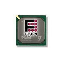
AFS250-FGG256 Actel, AFS250-FGG256 Datasheet - Page 115

AFS250-FGG256
Manufacturer Part Number
AFS250-FGG256
Description
FPGA - Field Programmable Gate Array 250K System Gates
Manufacturer
Actel
Datasheet
1.AFS600-PQG208.pdf
(330 pages)
Specifications of AFS250-FGG256
Processor Series
AFS250
Core
IP Core
Maximum Operating Frequency
1098.9 MHz
Number Of Programmable I/os
114
Data Ram Size
36864
Supply Voltage (max)
1.575 V
Maximum Operating Temperature
+ 70 C
Minimum Operating Temperature
0 C
Development Tools By Supplier
AFS-Eval-Kit, AFS-BRD600, FlashPro 3, FlashPro Lite, Silicon-Explorer II, Silicon-Sculptor 3, SI-EX-TCA
Mounting Style
SMD/SMT
Supply Voltage (min)
1.425 V
Number Of Gates
250 K
Package / Case
FPBGA-256
Lead Free Status / RoHS Status
Lead free / RoHS Compliant
Available stocks
Company
Part Number
Manufacturer
Quantity
Price
Company:
Part Number:
AFS250-FGG256
Manufacturer:
Actel
Quantity:
135
Company:
Part Number:
AFS250-FGG256
Manufacturer:
ACTEL
Quantity:
6 800
Company:
Part Number:
AFS250-FGG256I
Manufacturer:
Microsemi SoC
Quantity:
10 000
- Current page: 115 of 330
- Download datasheet (13Mb)
Actel Fusion Family of Mixed Signal FPGAs
Terminology
Resolution
Resolution defines the smallest temperature change Fusion Temperature Monitor can resolve. For ADC
configured as 8-bit mode, each LSB represents 4°C, and 1°C per LSB for 10-bit mode. With 12-bit mode,
the Temperature Monitor can still only resolve 1°C due to Temperature Monitor design.
Offset
The Fusion Temperature Monitor has a systematic offset of +5°C, excluding error due board resistance
and ideality factor of the external diode, between the operation range of –40°C to +85°C. For instance,
25°C will be read by the Temperature Monitor as 30°C plus error. The user can remove any offset error
through hardware or software during the calibration routine.
Analog-to-Digital Converter Block
At the heart of the Fusion analog system is a programmable Successive Approximation Register (SAR)
ADC. The ADC can support 8-, 10-, or 12-bit modes of operation. In 12-bit mode, the ADC can resolve
500 ksps. All results are MSB-justified in the ADC. The input to the ADC is a large 32:1 analog input
multiplexer. A simplified block diagram of the Analog Quads, analog input multiplexer, and ADC is shown
in
Figure
2-80. The ADC offers multiple self-calibrating modes to ensure consistent high performance
both at power-up and during runtime.
R e v i s i o n 1
2- 99
Related parts for AFS250-FGG256
Image
Part Number
Description
Manufacturer
Datasheet
Request
R

Part Number:
Description:
FPGA 256/I�/Fusion Voltage: 1.5, 1.8, 2.5, 3.3 Mixed Voltage
Manufacturer:
Actel
Datasheet:

Part Number:
Description:
FPGA - Field Programmable Gate Array 250K System Gates
Manufacturer:
Actel
Datasheet:

Part Number:
Description:
MCU, MPU & DSP Development Tools Silicon Sculptor Programming Mod
Manufacturer:
Actel

Part Number:
Description:
MCU, MPU & DSP Development Tools InSystem Programming ProASICPLUS Devices
Manufacturer:
Actel

Part Number:
Description:
Programming Socket Adapters & Emulators PQ160 Module
Manufacturer:
Actel

Part Number:
Description:
Programming Socket Adapters & Emulators Axcelerator Adap Module Kit
Manufacturer:
Actel

Part Number:
Description:
Programming Socket Adapters & Emulators Evaluation
Manufacturer:
Actel

Part Number:
Description:
Programming Socket Adapters & Emulators AFDX Solutions
Manufacturer:
Actel

Part Number:
Description:
Programming Socket Adapters & Emulators SILICON SCULPTOR ADAPTER MODULE
Manufacturer:
Actel
Datasheet:

Part Number:
Description:
Programming Socket Adapters & Emulators Axcelerator Adap Module Kit
Manufacturer:
Actel

Part Number:
Description:
Programming Socket Adapters & Emulators Evaluation
Manufacturer:
Actel

Part Number:
Description:
Programming Socket Adapters & Emulators Silicon Sculptor Software
Manufacturer:
Actel

Part Number:
Description:
Programming Socket Adapters & Emulators InSystem Programming ProASICPLUS Devices
Manufacturer:
Actel


