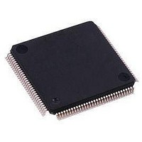
AT91SAM7SE256B-AUR Atmel, AT91SAM7SE256B-AUR Datasheet - Page 566

AT91SAM7SE256B-AUR
Manufacturer Part Number
AT91SAM7SE256B-AUR
Description
IC ARM7 MCU FLASH 256K 128-LQFP
Manufacturer
Atmel
Series
AT91SAMr
Datasheet
1.AT91SAM7SE256-AU.pdf
(673 pages)
Specifications of AT91SAM7SE256B-AUR
Core Processor
ARM7
Core Size
16/32-Bit
Speed
55MHz
Connectivity
EBI/EMI, I²C, SPI, SSC, UART/USART, USB
Peripherals
Brown-out Detect/Reset, POR, PWM, WDT
Number Of I /o
88
Program Memory Size
256KB (256K x 8)
Program Memory Type
FLASH
Ram Size
32K x 8
Voltage - Supply (vcc/vdd)
1.65 V ~ 1.95 V
Data Converters
A/D 8x10b
Oscillator Type
Internal
Operating Temperature
-40°C ~ 85°C
Package / Case
*
Processor Series
SAM7SE256
Core
ARM7TDMI
Data Bus Width
32 bit
Data Ram Size
32 KB
Interface Type
SPI, USB
Maximum Clock Frequency
48 MHz
Number Of Programmable I/os
88
Maximum Operating Temperature
+ 85 C
Mounting Style
SMD/SMT
Operating Temperature Range
- 40 C to + 85 C
Processor To Be Evaluated
AT91SAM7SE256B
Supply Current (max)
60 uA
Lead Free Status / RoHS Status
Lead free / RoHS Compliant
Eeprom Size
-
Lead Free Status / Rohs Status
Details
Available stocks
Company
Part Number
Manufacturer
Quantity
Price
- Current page: 566 of 673
- Download datasheet (11Mb)
38.5.2.7
Figure 38-10. Bank Swapping in Data OUT Transfers for Ping-pong Endpoints
566
SAM7SE512/256/32 Preliminary
Using Endpoints With Ping-pong Attributes
1 st Data Payload
2 nd Data Payload
3 rd Data Payload
Microcontroller
Write and Read at the Same Time
During isochronous transfer, using an endpoint with ping-pong attributes is obligatory. To be
able to guarantee a constant bandwidth, the microcontroller must read the previous data pay-
load sent by the host, while the current data payload is received by the USB device. Thus two
banks of memory are used. While one is available for the microcontroller, the other one is locked
by the USB device.
When using a ping-pong endpoint, the following procedures are required to perform Data OUT
transactions:
1. The host generates a Data OUT packet.
2. This packet is received by the USB device endpoint. It is written in the endpoint’s FIFO
3. The USB device sends an ACK PID packet to the host. The host can immediately send
4. The microcontroller is notified that the USB device has received a data payload, polling
5. The number of bytes available in the FIFO is made available by reading RXBYTECNT
6. The microcontroller transfers out data received from the endpoint’s memory to the
7. The microcontroller notifies the USB peripheral device that it has finished the transfer
8. A third Data OUT packet can be accepted by the USB peripheral device and copied in
9. If a second Data OUT packet has been received, the microcontroller is notified by the
Bank 0.
a second Data OUT packet. It is accepted by the device and copied to FIFO Bank 1.
RX_DATA_BK0 in the endpoint’s UDP_CSRx register. An interrupt is pending for this
endpoint while RX_DATA_BK0 is set.
in the endpoint’s UDP_CSRx register.
microcontroller’s memory. Data received is made available by reading the endpoint’s
UDP_FDRx register.
by clearing RX_DATA_BK0 in the endpoint’s UDP_CSRx register.
the FIFO Bank 0.
flag RX_DATA_BK1 set in the endpoint’s UDP_CSRx register. An interrupt is pending
for this endpoint while RX_DATA_BK1 is set.
Bank 0
Endpoint 1
Bank 1
Endpoint 1
Bank 0
Endpoint 1
Write
USB Device
Bank 0
Endpoint 1
Bank 1
Endpoint 1
Bank 0
Endpoint 1
Read
USB Bus
2 nd Data Payload
3 rd Data Payload
1 st Data Payload
Data IN Packet
Data IN Packet
Data IN Packet
6222F–ATARM–14-Jan-11
Related parts for AT91SAM7SE256B-AUR
Image
Part Number
Description
Manufacturer
Datasheet
Request
R

Part Number:
Description:
EVAL BOARD FOR AT91SAM7SE
Manufacturer:
Atmel
Datasheet:

Part Number:
Description:
DEV KIT FOR AVR/AVR32
Manufacturer:
Atmel
Datasheet:

Part Number:
Description:
INTERVAL AND WIPE/WASH WIPER CONTROL IC WITH DELAY
Manufacturer:
ATMEL Corporation
Datasheet:

Part Number:
Description:
Low-Voltage Voice-Switched IC for Hands-Free Operation
Manufacturer:
ATMEL Corporation
Datasheet:

Part Number:
Description:
MONOLITHIC INTEGRATED FEATUREPHONE CIRCUIT
Manufacturer:
ATMEL Corporation
Datasheet:

Part Number:
Description:
AM-FM Receiver IC U4255BM-M
Manufacturer:
ATMEL Corporation
Datasheet:

Part Number:
Description:
Monolithic Integrated Feature Phone Circuit
Manufacturer:
ATMEL Corporation
Datasheet:

Part Number:
Description:
Multistandard Video-IF and Quasi Parallel Sound Processing
Manufacturer:
ATMEL Corporation
Datasheet:

Part Number:
Description:
High-performance EE PLD
Manufacturer:
ATMEL Corporation
Datasheet:

Part Number:
Description:
8-bit Flash Microcontroller
Manufacturer:
ATMEL Corporation
Datasheet:

Part Number:
Description:
2-Wire Serial EEPROM
Manufacturer:
ATMEL Corporation
Datasheet:


