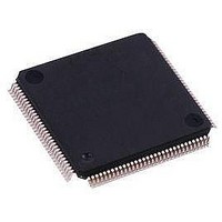
AT91SAM7SE256B-AUR Atmel, AT91SAM7SE256B-AUR Datasheet - Page 521

AT91SAM7SE256B-AUR
Manufacturer Part Number
AT91SAM7SE256B-AUR
Description
IC ARM7 MCU FLASH 256K 128-LQFP
Manufacturer
Atmel
Series
AT91SAMr
Datasheet
1.AT91SAM7SE256-AU.pdf
(673 pages)
Specifications of AT91SAM7SE256B-AUR
Core Processor
ARM7
Core Size
16/32-Bit
Speed
55MHz
Connectivity
EBI/EMI, I²C, SPI, SSC, UART/USART, USB
Peripherals
Brown-out Detect/Reset, POR, PWM, WDT
Number Of I /o
88
Program Memory Size
256KB (256K x 8)
Program Memory Type
FLASH
Ram Size
32K x 8
Voltage - Supply (vcc/vdd)
1.65 V ~ 1.95 V
Data Converters
A/D 8x10b
Oscillator Type
Internal
Operating Temperature
-40°C ~ 85°C
Package / Case
*
Processor Series
SAM7SE256
Core
ARM7TDMI
Data Bus Width
32 bit
Data Ram Size
32 KB
Interface Type
SPI, USB
Maximum Clock Frequency
48 MHz
Number Of Programmable I/os
88
Maximum Operating Temperature
+ 85 C
Mounting Style
SMD/SMT
Operating Temperature Range
- 40 C to + 85 C
Processor To Be Evaluated
AT91SAM7SE256B
Supply Current (max)
60 uA
Lead Free Status / RoHS Status
Lead free / RoHS Compliant
Eeprom Size
-
Lead Free Status / Rohs Status
Details
Available stocks
Company
Part Number
Manufacturer
Quantity
Price
- Current page: 521 of 673
- Download datasheet (11Mb)
36.6.6
Name:
Access:
• TCCLKS: Clock Selection
• CLKI: Clock Invert
0 = Counter is incremented on rising edge of the clock.
1 = Counter is incremented on falling edge of the clock.
• BURST: Burst Signal Selection
• LDBSTOP: Counter Clock Stopped with RB Loading
0 = Counter clock is not stopped when RB loading occurs.
1 = Counter clock is stopped when RB loading occurs.
• LDBDIS: Counter Clock Disable with RB Loading
0 = Counter clock is not disabled when RB loading occurs.
1 = Counter clock is disabled when RB loading occurs.
6222F–ATARM–14-Jan-11
WAVE = 0
LDBDIS
31
23
15
–
–
7
0
0
0
0
1
1
1
1
0
0
1
1
TC Channel Mode Register: Capture Mode
BURST
LDBSTOP
CPCTRG
30
22
14
TC_CMR
Read/Write
–
–
6
TCCLKS
0
1
0
1
0
0
1
1
0
0
1
1
The clock is not gated by an external signal.
XC0 is ANDed with the selected clock.
XC1 is ANDed with the selected clock.
XC2 is ANDed with the selected clock.
29
21
13
–
–
–
5
BURST
0
1
0
1
0
1
0
1
28
20
12
–
–
–
4
Clock Selected
TIMER_CLOCK1
TIMER_CLOCK2
TIMER_CLOCK3
TIMER_CLOCK4
TIMER_CLOCK5
XC0
XC1
XC2
SAM7SE512/256/32 Preliminary
CLKI
27
19
11
–
–
3
LDRB
ABETRG
26
18
10
–
2
TCCLKS
25
17
–
9
1
ETRGEDG
LDRA
24
16
–
8
0
521
Related parts for AT91SAM7SE256B-AUR
Image
Part Number
Description
Manufacturer
Datasheet
Request
R

Part Number:
Description:
EVAL BOARD FOR AT91SAM7SE
Manufacturer:
Atmel
Datasheet:

Part Number:
Description:
DEV KIT FOR AVR/AVR32
Manufacturer:
Atmel
Datasheet:

Part Number:
Description:
INTERVAL AND WIPE/WASH WIPER CONTROL IC WITH DELAY
Manufacturer:
ATMEL Corporation
Datasheet:

Part Number:
Description:
Low-Voltage Voice-Switched IC for Hands-Free Operation
Manufacturer:
ATMEL Corporation
Datasheet:

Part Number:
Description:
MONOLITHIC INTEGRATED FEATUREPHONE CIRCUIT
Manufacturer:
ATMEL Corporation
Datasheet:

Part Number:
Description:
AM-FM Receiver IC U4255BM-M
Manufacturer:
ATMEL Corporation
Datasheet:

Part Number:
Description:
Monolithic Integrated Feature Phone Circuit
Manufacturer:
ATMEL Corporation
Datasheet:

Part Number:
Description:
Multistandard Video-IF and Quasi Parallel Sound Processing
Manufacturer:
ATMEL Corporation
Datasheet:

Part Number:
Description:
High-performance EE PLD
Manufacturer:
ATMEL Corporation
Datasheet:

Part Number:
Description:
8-bit Flash Microcontroller
Manufacturer:
ATMEL Corporation
Datasheet:

Part Number:
Description:
2-Wire Serial EEPROM
Manufacturer:
ATMEL Corporation
Datasheet:


