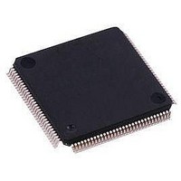
AT91SAM7SE256B-AUR Atmel, AT91SAM7SE256B-AUR Datasheet - Page 107

AT91SAM7SE256B-AUR
Manufacturer Part Number
AT91SAM7SE256B-AUR
Description
IC ARM7 MCU FLASH 256K 128-LQFP
Manufacturer
Atmel
Series
AT91SAMr
Datasheet
1.AT91SAM7SE256-AU.pdf
(673 pages)
Specifications of AT91SAM7SE256B-AUR
Core Processor
ARM7
Core Size
16/32-Bit
Speed
55MHz
Connectivity
EBI/EMI, I²C, SPI, SSC, UART/USART, USB
Peripherals
Brown-out Detect/Reset, POR, PWM, WDT
Number Of I /o
88
Program Memory Size
256KB (256K x 8)
Program Memory Type
FLASH
Ram Size
32K x 8
Voltage - Supply (vcc/vdd)
1.65 V ~ 1.95 V
Data Converters
A/D 8x10b
Oscillator Type
Internal
Operating Temperature
-40°C ~ 85°C
Package / Case
*
Processor Series
SAM7SE256
Core
ARM7TDMI
Data Bus Width
32 bit
Data Ram Size
32 KB
Interface Type
SPI, USB
Maximum Clock Frequency
48 MHz
Number Of Programmable I/os
88
Maximum Operating Temperature
+ 85 C
Mounting Style
SMD/SMT
Operating Temperature Range
- 40 C to + 85 C
Processor To Be Evaluated
AT91SAM7SE256B
Supply Current (max)
60 uA
Lead Free Status / RoHS Status
Lead free / RoHS Compliant
Eeprom Size
-
Lead Free Status / Rohs Status
Details
Available stocks
Company
Part Number
Manufacturer
Quantity
Price
- Current page: 107 of 673
- Download datasheet (11Mb)
Figure 19-6. Example of Partial Page Programming:
19.2.4.2
6222F–ATARM–14-Jan-11
16 words
16 words
16 words
16 words
Erase All Command
FF
FF
FF
FF
FF
FF
FF
FF
FF
FF
FF
FF
Erase All Flash
Page 7 erased
32 bits wide
Step 1.
FF
FF
FF
FF
FF
FF
FF
FF
FF
FF
FF
FF
...
...
...
...
FF
FF
FF
FF
FF
FF
FF
FF
FF
FF
FF
FF
The Partial Programming mode works only with 32-bit (or higher) boundaries. It cannot be used
with boundaries lower than 32 bits (8 or 16-bit for example).
After programming, the page (the whole lock region) can be locked to prevent miscellaneous
write or erase sequences. The lock bit can be automatically set after page programming using
WPL.
Data to be written is stored in an internal latch buffer. The size of the latch buffer corresponds to
the page size. The latch buffer wraps around within the internal memory area address space
and appears to be repeated by the number of pages in it.
Note:
Data is written to the latch buffer before the programming command is written to the Flash Com-
mand Register MC_FCR. The sequence is as follows:
Two errors can be detected in the MC_FSR register after a programming sequence:
The entire memory can be erased if the Erase All Command (EA) in the Flash Command Regis-
ter MC_FCR is written.
• Write the full page, at any page address, within the internal memory area address space
• Programming starts as soon as the page number and the programming command are written
• When programming is completed, the bit FRDY in the Flash Programming Status Register
• Programming Error: A bad keyword and/or an invalid command have been written in the
• Lock Error: The page to be programmed belongs to a locked region. A command must be
FF
FF
FF
FF
FF
FF
FF
FF
FF
FF
FF
FF
using only 32-bit access.
to the Flash Command Register. The FRDY bit in the Flash Programming Status Register
(MC_FSR) is automatically cleared.
(MC_FSR) rises. If an interrupt was enabled by setting the bit FRDY in MC_FMR, the
interrupt line of the Memory Controller is activated.
MC_FCR register.
previously run to unlock the corresponding region.
Writing of 8-bit and 16-bit data is not allowed and may lead to unpredictable data corruption.
Programming of the second part of Page 7
FF
FF
FF
CA FE
CA FE
CA FE
FF
FF
FF
FF
FF
FF
(NEBP = 1)
32 bits wide
FF
FF
FF
FF
FF
FF
FF
FF
FF
Step 2.
...
...
...
...
SAM7SE512/256/32 Preliminary
CA
CA
CA
FF
FF
FF
FF
FF
FF
FF
FF
FF
FF
FF
FF
FF
FF
FF
FF
FF
FF
FE
FE
FE
Programming of the third part of Page 7
CA FE
CA FE
CA FE
FF
FF
FF
DE CA
DE CA
DE CA
FF
FF
FF
(NEBP = 1)
32 bits wide
FF
FF
FF
FF
FF
FF
Step 3.
...
...
...
...
CA
CA
CA
FF
FF
FF
DE CA
DE CA
DE CA
FF
FF
FF
FF
FF
FF
FE
FE
FE
FF
FF
FF
107
Related parts for AT91SAM7SE256B-AUR
Image
Part Number
Description
Manufacturer
Datasheet
Request
R

Part Number:
Description:
EVAL BOARD FOR AT91SAM7SE
Manufacturer:
Atmel
Datasheet:

Part Number:
Description:
DEV KIT FOR AVR/AVR32
Manufacturer:
Atmel
Datasheet:

Part Number:
Description:
INTERVAL AND WIPE/WASH WIPER CONTROL IC WITH DELAY
Manufacturer:
ATMEL Corporation
Datasheet:

Part Number:
Description:
Low-Voltage Voice-Switched IC for Hands-Free Operation
Manufacturer:
ATMEL Corporation
Datasheet:

Part Number:
Description:
MONOLITHIC INTEGRATED FEATUREPHONE CIRCUIT
Manufacturer:
ATMEL Corporation
Datasheet:

Part Number:
Description:
AM-FM Receiver IC U4255BM-M
Manufacturer:
ATMEL Corporation
Datasheet:

Part Number:
Description:
Monolithic Integrated Feature Phone Circuit
Manufacturer:
ATMEL Corporation
Datasheet:

Part Number:
Description:
Multistandard Video-IF and Quasi Parallel Sound Processing
Manufacturer:
ATMEL Corporation
Datasheet:

Part Number:
Description:
High-performance EE PLD
Manufacturer:
ATMEL Corporation
Datasheet:

Part Number:
Description:
8-bit Flash Microcontroller
Manufacturer:
ATMEL Corporation
Datasheet:

Part Number:
Description:
2-Wire Serial EEPROM
Manufacturer:
ATMEL Corporation
Datasheet:


