AT91SAM7SE256B-AUR Atmel, AT91SAM7SE256B-AUR Datasheet - Page 468
AT91SAM7SE256B-AUR
Manufacturer Part Number
AT91SAM7SE256B-AUR
Description
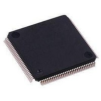
IC ARM7 MCU FLASH 256K 128-LQFP
Manufacturer
Atmel
Series
AT91SAMr
Datasheet
1.AT91SAM7SE256-AU.pdf
(673 pages)
Specifications of AT91SAM7SE256B-AUR
Core Processor
ARM7
Core Size
16/32-Bit
Speed
55MHz
Connectivity
EBI/EMI, I²C, SPI, SSC, UART/USART, USB
Peripherals
Brown-out Detect/Reset, POR, PWM, WDT
Number Of I /o
88
Program Memory Size
256KB (256K x 8)
Program Memory Type
FLASH
Ram Size
32K x 8
Voltage - Supply (vcc/vdd)
1.65 V ~ 1.95 V
Data Converters
A/D 8x10b
Oscillator Type
Internal
Operating Temperature
-40°C ~ 85°C
Package / Case
*
Processor Series
SAM7SE256
Core
ARM7TDMI
Data Bus Width
32 bit
Data Ram Size
32 KB
Interface Type
SPI, USB
Maximum Clock Frequency
48 MHz
Number Of Programmable I/os
88
Maximum Operating Temperature
+ 85 C
Mounting Style
SMD/SMT
Operating Temperature Range
- 40 C to + 85 C
Processor To Be Evaluated
AT91SAM7SE256B
Supply Current (max)
60 uA
Lead Free Status / RoHS Status
Lead free / RoHS Compliant
Eeprom Size
-
Lead Free Status / Rohs Status
Details
Available stocks
Company
Part Number
Manufacturer
Quantity
Price


35.6.1.3
468
SAM7SE512/256/32 Preliminary
Receiver Clock Management
The transmitter can also drive the TK I/O pad continuously or be limited to the actual data trans-
fer. The clock output is configured by the SSC_TCMR register. The Transmit Clock Inversion
(CKI) bits have no effect on the clock outputs. Programming the TCMR register to select TK pin
(CKS field) and at the same time Continuous Transmit Clock (CKO field) might lead to unpredict-
able results.
Figure 35-6. Transmitter Clock Management
The receiver clock is generated from the transmitter clock or the divider clock or an external
clock scanned on the RK I/O pad. The Receive Clock is selected by the CKS field in
SSC_RCMR (Receive Clock Mode Register). Receive Clocks can be inverted independently by
the CKI bits in SSC_RCMR.
The receiver can also drive the RK I/O pad continuously or be limited to the actual data transfer.
The clock output is configured by the SSC_RCMR register. The Receive Clock Inversion (CKI)
bits have no effect on the clock outputs. Programming the RCMR register to select RK pin (CKS
field) and at the same time Continuous Receive Clock (CKO field) can lead to unpredictable
results.
Receiver
TK (pin)
Divider
Clock
Clock
MUX
CKS
CKO
Controller
Tri_state
MUX
INV
CKI
Data Transfer
Controller
Tri-state
CKG
6222F–ATARM–14-Jan-11
Transmitter
Clock
Clock
Output
Related parts for AT91SAM7SE256B-AUR
Image
Part Number
Description
Manufacturer
Datasheet
Request
R

Part Number:
Description:
EVAL BOARD FOR AT91SAM7SE
Manufacturer:
Atmel
Datasheet:

Part Number:
Description:
DEV KIT FOR AVR/AVR32
Manufacturer:
Atmel
Datasheet:

Part Number:
Description:
INTERVAL AND WIPE/WASH WIPER CONTROL IC WITH DELAY
Manufacturer:
ATMEL Corporation
Datasheet:
Part Number:
Description:
Low-Voltage Voice-Switched IC for Hands-Free Operation
Manufacturer:
ATMEL Corporation
Datasheet:
Part Number:
Description:
MONOLITHIC INTEGRATED FEATUREPHONE CIRCUIT
Manufacturer:
ATMEL Corporation
Datasheet:
Part Number:
Description:
AM-FM Receiver IC U4255BM-M
Manufacturer:
ATMEL Corporation
Datasheet:
Part Number:
Description:
Monolithic Integrated Feature Phone Circuit
Manufacturer:
ATMEL Corporation
Datasheet:
Part Number:
Description:
Multistandard Video-IF and Quasi Parallel Sound Processing
Manufacturer:
ATMEL Corporation
Datasheet:
Part Number:
Description:
High-performance EE PLD
Manufacturer:
ATMEL Corporation
Datasheet:
Part Number:
Description:
8-bit Flash Microcontroller
Manufacturer:
ATMEL Corporation
Datasheet:
Part Number:
Description:
2-Wire Serial EEPROM
Manufacturer:
ATMEL Corporation
Datasheet: