DR-TRC104-2400-DK RFM, DR-TRC104-2400-DK Datasheet - Page 28
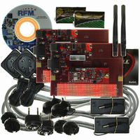
DR-TRC104-2400-DK
Manufacturer Part Number
DR-TRC104-2400-DK
Description
KIT DEV FOR TRC104
Manufacturer
RFM
Type
Transceiverr
Datasheets
1.DR-TRC104-2400-DK.pdf
(33 pages)
2.DR-TRC104-2400-DK.pdf
(1 pages)
3.DR-TRC104-2400-DK.pdf
(2 pages)
Specifications of DR-TRC104-2400-DK
Frequency
2.4GHz
For Use With/related Products
TRC104
Lead Free Status / RoHS Status
Lead free / RoHS Compliant
Other names
583-1137


8.14 Analog Turn-On Control
0x15 [default 0XB4]
8.15 Reserved
Do not write to configuration register address 0x16. It should retain its power-on default value.
8.16 Option Control
0x17 – [default 22h]
Address
8.17 Reserved
Do not write to configuration registers addresses 0x18 and higher, except as discussed in Section 8.18.
8.18 Default Overrides for Enhanced Performance
TRC104 operation can be enhanced by overriding several default values in register addresses shown in Table 38.
These override values should be written before the TRC104 is first placed in a transmit or receive mode.
www.RFM.com
©2009 by RF Monolithics, Inc.
Address
0X15
0X17
Name
ANA_ON
Name
LVLINT
LVLDRSSI
E-mail:
-
-
-
info@rfm.com
Bits
7..6
5..4
3..0
Bits
Register Address
7..2
1
0
0X2C
0X06
0X39
0X4F
0X77
R/W
R/W
r/w
r/w
r/w
r/w
r/w
r/w
Description
Reserved, always set to 10b
Analog circuitry turn-on time (Burst Mode only):
Reserved, always set to 0100b
Description
Reserved, always set to 0010 00b
Active edge for INT pin (Burst Mode only):
Active edge for DRSSI pin (Continuous Mode only):
Technical support +1.800.704.6079
00 → 0 µs
01 → 10 µs
10 → 20 µs
11 → 40 µs
Note: default value is suitable for most applications
0 → Falling edge active (active low)
1 → Rising edge active (active high)
0 → Falling edge active (active low)
1 → Rising edge active (active high)
Power-on Default
Table 36
Table 37
Table 38
0XBB
0X7C
0X30
0X19
0X26
Default Override
0XB0
0XB9
0X5C
0X18
0X66
TRC104 - 08/13/09
Page 28 of 33
Related parts for DR-TRC104-2400-DK
Image
Part Number
Description
Manufacturer
Datasheet
Request
R

Part Number:
Description:
ASH RX 115.2 KBPS 433.92 MHZ
Manufacturer:
RFM
Datasheet:

Part Number:
Description:
RFIC TRANCEIVER MULTI-CHANNEL FS
Manufacturer:
RFM
Datasheet:

Part Number:
Description:
ASH TX 115.2 KBPS 433.92 MHZ
Manufacturer:
RFM
Datasheet:
Part Number:
Description:
Filters 1602MHz BW=61MHz
Manufacturer:
RFM
Datasheet:

Part Number:
Description:
RESONATOR, SM3030-6
Manufacturer:
RFM
Datasheet:

Part Number:
Description:
RESONATOR, SM3030-6
Manufacturer:
RFM
Datasheet:

Part Number:
Description:
RESONATOR, SM3030-6
Manufacturer:
RFM
Datasheet:

Part Number:
Description:
RESONATOR, SM5035-4
Manufacturer:
RFM
Datasheet:
Part Number:
Description:
RESONATOR 418MHZ SM5035-4
Manufacturer:
RFM
Datasheet:
Part Number:
Description:
RESONATOR 315 MHZ SMD
Manufacturer:
RFM
Datasheet:
Part Number:
Description:
WiFi / 802.11 Modules 2.4 and 5.8GHz + BT
Manufacturer:
RFM
Datasheet:

Part Number:
Description:
10-Terminal Ceramic Surface-Mount Case 7 x 5 mm Nominal Footprint
Manufacturer:
RFM [RF Monolithics, Inc]
Datasheet:
Part Number:
Description:
QUAD-BAND GSM850/GSM/DCS/PCS POWER AMP MODULE
Manufacturer:
RFM [RF Monolithics, Inc]
Datasheet:
Part Number:
Description:
402 to 405 MHz Medical Band Front-end Filter
Manufacturer:
RFM [RF Monolithics, Inc]
Datasheet: