DR-TRC104-2400-DK RFM, DR-TRC104-2400-DK Datasheet - Page 10
DR-TRC104-2400-DK
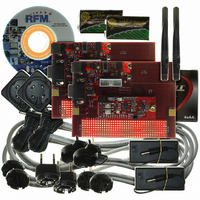
Manufacturer Part Number
DR-TRC104-2400-DK
Description
KIT DEV FOR TRC104
Manufacturer
RFM
Type
Transceiverr
Datasheets
1.DR-TRC104-2400-DK.pdf
(33 pages)
2.DR-TRC104-2400-DK.pdf
(1 pages)
3.DR-TRC104-2400-DK.pdf
(2 pages)
Specifications of DR-TRC104-2400-DK
Frequency
2.4GHz
For Use With/related Products
TRC104
Lead Free Status / RoHS Status
Lead free / RoHS Compliant
Other names
583-1137


3.3 PLL
The PLL channel is set with the Ch_Num bits in configuration register 0x00. In transmit mode, the PLL is normally
turned on with the falling edge of the MODE input. The TRC104 transmits the data after the PLL locks and the
power amplifier has ramped up to its programmed level. PLL lock time is typically 170 µs. It is possible to enable
and lock the PLL before the falling edge of MODE input. This can provides a shorter transition time to transmit.
The PLL pre-start delay time is adjustable from 20 µs up to 5 ms. The value of PLL_ON in register 0x14 sets this
time. The pre-start delay timer is triggered on the rising edge of MODE as shown in Figure 5. The value of
PLL_ON determines the delay time from the rising edge of MODE before the PLL is enabled. Care must be taken
to carefully calculate the write time of the data packet into the transmit FIFO so that the TRC104 does not enable
the transmitter and begin sending data before the data packet is fully written to the FIFO, in which case the
TRC104 will discard the current packet.
3.4 Crystal Oscillator
At the 1 Mb/s RF data rate, the TRC104 uses a 16 MHz crystal. At the 250 kb/s RF data rate, the TRC104 can
use any one of five standard crystal frequencies: 4, 8, 12, 16, or 20 MHz. The crystal frequency is configured by
setting the FXTAL bits in register 0x01. At the 250 kb/s data rate, the TRC104’s power consumption is reduced by
using one of the lower crystal frequencies. The total load capacitance C
terminals is composed primarily of C
A typical value for C
C
www.RFM.com
©2009 by RF Monolithics, Inc.
L
matches the load capacitance specified for the crystal. A typical C
C
L
= 1/((1/C
E-mail:
info@rfm.com
IN
STRAY
) + (1/C
is 1 pF. The values of C
OUT
) ) + C
IN
and C
STRAY
, where C
Technical support +1.800.704.6079
OUT
in series, as shown if Figure 6:
IN
and C
Figure 5
Figure 6
STRAY
OUT
is the capacitance associated with the PCB layout
should be approximately equal and chosen so that
L
value for a 16 MHz crystal is 12 pF. The
L
seen between the XTLIN and XTLOUT
TRC104 - 08/13/09
Page 10 of 33
Related parts for DR-TRC104-2400-DK
Image
Part Number
Description
Manufacturer
Datasheet
Request
R

Part Number:
Description:
ASH RX 115.2 KBPS 433.92 MHZ
Manufacturer:
RFM
Datasheet:

Part Number:
Description:
RFIC TRANCEIVER MULTI-CHANNEL FS
Manufacturer:
RFM
Datasheet:

Part Number:
Description:
ASH TX 115.2 KBPS 433.92 MHZ
Manufacturer:
RFM
Datasheet:
Part Number:
Description:
Filters 1602MHz BW=61MHz
Manufacturer:
RFM
Datasheet:

Part Number:
Description:
RESONATOR, SM3030-6
Manufacturer:
RFM
Datasheet:

Part Number:
Description:
RESONATOR, SM3030-6
Manufacturer:
RFM
Datasheet:

Part Number:
Description:
RESONATOR, SM3030-6
Manufacturer:
RFM
Datasheet:

Part Number:
Description:
RESONATOR, SM5035-4
Manufacturer:
RFM
Datasheet:
Part Number:
Description:
RESONATOR 418MHZ SM5035-4
Manufacturer:
RFM
Datasheet:
Part Number:
Description:
RESONATOR 315 MHZ SMD
Manufacturer:
RFM
Datasheet:
Part Number:
Description:
WiFi / 802.11 Modules 2.4 and 5.8GHz + BT
Manufacturer:
RFM
Datasheet:

Part Number:
Description:
10-Terminal Ceramic Surface-Mount Case 7 x 5 mm Nominal Footprint
Manufacturer:
RFM [RF Monolithics, Inc]
Datasheet:
Part Number:
Description:
QUAD-BAND GSM850/GSM/DCS/PCS POWER AMP MODULE
Manufacturer:
RFM [RF Monolithics, Inc]
Datasheet:
Part Number:
Description:
402 to 405 MHz Medical Band Front-end Filter
Manufacturer:
RFM [RF Monolithics, Inc]
Datasheet: