DR-TRC104-2400-DK RFM, DR-TRC104-2400-DK Datasheet - Page 16
DR-TRC104-2400-DK
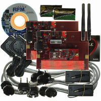
Manufacturer Part Number
DR-TRC104-2400-DK
Description
KIT DEV FOR TRC104
Manufacturer
RFM
Type
Transceiverr
Datasheets
1.DR-TRC104-2400-DK.pdf
(33 pages)
2.DR-TRC104-2400-DK.pdf
(1 pages)
3.DR-TRC104-2400-DK.pdf
(2 pages)
Specifications of DR-TRC104-2400-DK
Frequency
2.4GHz
For Use With/related Products
TRC104
Lead Free Status / RoHS Status
Lead free / RoHS Compliant
Other names
583-1137


0x09 - 0x0D, or by writing it directly before the payload data bytes. The source for the destination address is
chosen by the DesADD_ref bit in configuration register 0x05. When writing the destination address directly, the
most significant address byte is written first. Sender (local device) addressing is optional. If used, the sender
address is automatically loaded from configuration registers 0x0E - 0x12. The destination address can be from
one to five bytes in length. If used, the sender address must be the same length as the destination address.
5.2.2 Burst Receive Mode
Burst Receive Mode is enabled when the C_Mode bit of register 0x00 is set to 0 and the D_Mode bit of register
0x02 is set to 1. In Burst Receive Mode, the FIFO is loaded with the payload data part of a received packet. The
automatic packet features listed in Section 5.2 are available for use in Burst Receive Mode. Using these features
frees up the host microcontroller to perform other tasks.
As a packet is received, the TRC104 uses the preamble to lock to the incoming data rate and then determines if
the packet is for it by testing the address following the preamble for a match to its own device address. If the
addresses match, the TRC104 receives the remainder of the packet, including the sender address if present, the
payload data and CRC. The TRC104 then performs a CRC calculation and compares the result with the received
CRC value. If the CRC’s match, the INT flag is asserted according to the interrupt polarity as configured by the
LVLINT bit of configuration register 0x17. Otherwise, the packet is discarded unless this default is overridden.
Upon assertion of the INT flag, the host microcontroller clocks out and discards two dummy bits, and then clocks
out received bits, checking the INT flag after each group of 8 bits. The INT flag will de-assert when the next-to-last
payload data byte in the FIFO is read. The host microcontroller then completes the read transaction by clocking
out the last FIFO byte followed by clocking out and discarding three more dummy bits. When the INT flag is
asserted the host microcontroller should read the data quickly so as not to delay listening for the next packet. If
the data has not been completely read when the next packet is transmitted, reception will not occur and the
transmitted data will be missed. Figure 14 and Table 13 show the serial port timing parameters for Burst Receive
Mode.
www.RFM.com
©2009 by RF Monolithics, Inc.
E-mail:
info@rfm.com
Item
T1
T2
T3
T4
T5
T6
Description
MODE to 1
SCLK Cycle Time
Setup Time
Hold Time
Address & Payload Data
Dummy Bit Writes
Technical support +1.800.704.6079
st
Bit Time
Figure 13
Table 12
Min
500
20
8
Typ
15
15
Max
296
3
Unit
bits
bits
µs
ns
ns
ns
TRC104 - 08/13/09
Page 16 of 33
Related parts for DR-TRC104-2400-DK
Image
Part Number
Description
Manufacturer
Datasheet
Request
R

Part Number:
Description:
ASH RX 115.2 KBPS 433.92 MHZ
Manufacturer:
RFM
Datasheet:

Part Number:
Description:
RFIC TRANCEIVER MULTI-CHANNEL FS
Manufacturer:
RFM
Datasheet:

Part Number:
Description:
ASH TX 115.2 KBPS 433.92 MHZ
Manufacturer:
RFM
Datasheet:
Part Number:
Description:
Filters 1602MHz BW=61MHz
Manufacturer:
RFM
Datasheet:

Part Number:
Description:
RESONATOR, SM3030-6
Manufacturer:
RFM
Datasheet:

Part Number:
Description:
RESONATOR, SM3030-6
Manufacturer:
RFM
Datasheet:

Part Number:
Description:
RESONATOR, SM3030-6
Manufacturer:
RFM
Datasheet:

Part Number:
Description:
RESONATOR, SM5035-4
Manufacturer:
RFM
Datasheet:
Part Number:
Description:
RESONATOR 418MHZ SM5035-4
Manufacturer:
RFM
Datasheet:
Part Number:
Description:
RESONATOR 315 MHZ SMD
Manufacturer:
RFM
Datasheet:
Part Number:
Description:
WiFi / 802.11 Modules 2.4 and 5.8GHz + BT
Manufacturer:
RFM
Datasheet:

Part Number:
Description:
10-Terminal Ceramic Surface-Mount Case 7 x 5 mm Nominal Footprint
Manufacturer:
RFM [RF Monolithics, Inc]
Datasheet:
Part Number:
Description:
QUAD-BAND GSM850/GSM/DCS/PCS POWER AMP MODULE
Manufacturer:
RFM [RF Monolithics, Inc]
Datasheet:
Part Number:
Description:
402 to 405 MHz Medical Band Front-end Filter
Manufacturer:
RFM [RF Monolithics, Inc]
Datasheet: