DR-TRC104-2400-DK RFM, DR-TRC104-2400-DK Datasheet
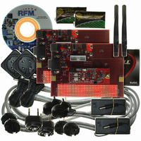
DR-TRC104-2400-DK
Specifications of DR-TRC104-2400-DK


Related parts for DR-TRC104-2400-DK


DR-TRC104-2400-DK Summary of contents
Page 1
... Programmable RF output power • 32-byte Transmit/receive FIFO • Programmable TX/RX FIFO depth • Continuous & protocol modes • Packet destination and sender addressing • Packet handling features - Packet address filtering Error detection • SPI configuration & data interface • TTL/CMOS compatible I/O pins • ...
Page 2
... RSSI Function Control .................................................................................................................... 23 8.5 RSSI Value ..................................................................................................................................... 24 8.6 Data Format Control ....................................................................................................................... 24 8.7 Preamble Control ............................................................................................................................ 25 8.8 Transmitter Rise/Fall Time Control ................................................................................................. 25 8.9 Address Length Control .................................................................................................................. 26 8.10 Destination Address...................................................................................................................... 26 8.11 Sender (Local Device) Address .................................................................................................... 27 8.12 Reserved....................................................................................................................................... 27 www.RFM.com E-mail: info@rfm.com ©2009 by RF Monolithics, Inc. Table of Contents Technical support +1 ...
Page 3
... Burst Packet Mode Serial Port Message Examples .............................................................................. 32 10.1 Destination Address from Configuration Registers, No Sender Address ..................................... 32 10.2 Destination Address Written by Host, No Sender Address .......................................................... 32 10.3 Destination and Sender Addresses from Configuration Registers ............................................... 32 10.4 Destination Address Written by Host, Sender Address from Configuration Register................... 32 11 Package Dimensions.............................................................................................................................. 33 www.RFM.com E-mail: info@rfm.com © ...
Page 4
... CS 5 VCCD 6 GNDD 7 VDDD 8 O XTLOUT 9 I XTLIN 10 I PMODE 11 GNDVCO 12 VCCVCO 13 VDDRF 14 RFIO RF+ 15 RFIO RF- 16 GNDRF 17 VCCRF 18 GNDIF 19 O RSSIA INT 22 O RSSID DIE PAD www.RFM.com E-mail: info@rfm.com ©2009 by RF Monolithics, Inc. Figure 1 DESCRIPTION Operating mode select input - used with PMODE and CS ...
Page 5
... Operating Temperature OP 2.1 DC Electrical Characteristics Minimum/maximum values are valid over the recommended operating range Vcc = 1.9-3.6 V. Typical conditions: T The electrical specifications given below are valid when using an RFM XTL1021 or equivalent crystal. PARAMETER Sleep Mode Current Stop Mode Current Standby Mode Current ...
Page 6
... AC Electrical Characteristics Minimum/maximum values are valid over the recommended operating range Vcc = 1.9-3.6 V. Typical conditions: T The electrical specifications given below are valid when using an RFM XTL1021 or equivalent crystal. PARAMETER RF Input Impedance RF Input Power Receiver Bandwidth Receiver Sensitivity Blocking Immunity Co-channel Rejection ...
Page 7
... Crystal Oscillator Frequency PLL Lock Time PLL Step Resolution Crystal Load Capacitance Crystal Oscillator Start time Frequency Range www.RFM.com E-mail: info@rfm.com ©2009 by RF Monolithics, Inc. TIMING NOTES MIN oscillator & PLL running oscillator & PLL running serial command to RX bit serial command to TX bit ...
Page 8
... The differential RF port also provides common mode signal rejection to enhance receiver interference immunity. A simple L-C balun can be used to convert the differential port to a single-ended output to drive an unbalanced antenna, as shown in Figure 3. 3.2 Transmitter Power Amplifier The power amplifier controls the output power level of the transmitter. The power amplifier has four programmable power levels ...
Page 9
... The ramp-up/ramp-down function increases or decreases the output power stage-by-stage as specified by the PA_RU and PA_RD bits of register 0x07, respectively. Figure 4 shows the timing for the ramp-up/ramp-down. www.RFM.com E-mail: info@rfm.com ©2009 by RF Monolithics, Inc. Figure 3 Figure 4 Technical support +1.800.704.6079 ...
Page 10
... OUT A typical value for pF. The values of C STRAY C matches the load capacitance specified for the crystal. A typical C L www.RFM.com E-mail: info@rfm.com ©2009 by RF Monolithics, Inc. Figure 5 and C in series, as shown if Figure 6: IN OUT ) ) + C , where C is the capacitance associated with the PCB layout ...
Page 11
... IF frequency. The output of the first mixer is applied to the second-conversion I and Q mixers, which are driven by I and Q LO signals 1/8 the frequency of the first LO. The outputs of the I and Q mixers are processed MHz complex IF filter, which provides both band-pass filtering and Hilbert transform phasing between the I and Q channels ...
Page 12
... If the digital value is greater than the threshold value, the RSSID pin is asserted according to the configuration of the LVLDRSSI bit of register 0x17. If the LVLDRSSI bit is set to 1, the RSSID pin is asserted high, otherwise the pin is asserted low. The output state of the RSSID pin is disabled while MODE is asserted. The RSSI function is only available in continuous mode, as discussed below ...
Page 13
... This mode is enabled to load the transmit FIFO or receive data. The mode function, transmit or receive, is set before enabling this mode. The mode function is selected by the C_Mode bit in configuration register 0x00. See Section 5 for descriptions and timing of the various data transfer modes. www.RFM.com E-mail: info@rfm.com ©2009 by RF Monolithics, Inc. Figure 9 Figure 10 Technical support +1.800.704.6079 ...
Page 14
... Also for this mode the responsibility of the host microcontroller to maintain correct bit timing to an accuracy there is no bit clock output for transmit timing ...
Page 15
... Continuous Receive Mode operation. This address is configured by writing the address byte(s) into configuration registers 0x0E - 0x12, according to the address length specified by the ADDR_len bits in configuration register 0x08. The sender address is written least significant byte first, starting in register 0x0E. ...
Page 16
... As a packet is received, the TRC104 uses the preamble to lock to the incoming data rate and then determines if the packet is for it by testing the address following the preamble for a match to its own device address. If the addresses match, the TRC104 receives the remainder of the packet, including the sender address if present, the payload data and CRC. The TRC104 then performs a CRC calculation and compares the result with the received CRC value. If the CRC’ ...
Page 17
... In Burst Packet Mode, the following packet features are available : • Configurable FIFO length bytes • Configurable preamble length bits • Configurable address filtering • Configurable sender/destination address length bytes • Configurable sender (local device) address • Configurable destination address • Configurable DC-balanced data scrambling/descrambling • ...
Page 18
... All TRC104 radios in a network must use the same address length. The destination address is stripped off by the receiver and is not included in the read out from the FIFO. The sender address may be output before the payload data in a received packet. This feature is enabled through configuration register 0x05, bits 7 ...
Page 19
... SDAT pin with host microcontroller clocking on the SCLK pin. The CS pin state selects whether the FIFO (Burst Packet Mode only) or the internal configuration registers are accessed. www.RFM.com E-mail: info@rfm.com ©2009 by RF Monolithics, Inc. Figure 16 Figure 17 Technical support +1.800.704.6079 ...
Page 20
... The serial interface is enabled for read/write transactions with the configuration registers by holding the CS pin high. The CS pin must remain high during the transmission of both the address and data bytes or the data will be corrupted. Between each configuration register read/write transaction the serial interface must be reset by pulling the CS pin low ...
Page 21
... Burst Transmit Mode and Burst Receive Mode using the FIFO. 8 Configuration Registers The TRC104’s user configuration registers are mapped in the address range of 0x00 through 0x18. Sections 8.1 through 8.17 below provide the details for each configuration register. Power-up default settings for the configuration register bit and byte patterns are shown in bold ...
Page 22
... T/R Mode and Channel Frequency Control 0x00 [default 0x28] Address Name Bits C_Mode 7 0X00 Ch_Num 6..0 8.2 Transmitter Power and Crystal Frequency Control 0x01 [default 0x03] Address Name Bits - 7..5 PWR 4..3 0X01 FXTAL 2..0 www.RFM.com E-mail: info@rfm.com ©2009 by RF Monolithics, Inc. ...
Page 23
... Analog RSSI refresh control bit (Continuous Mode only): 0 → Do not refresh RSSI value r/w 1 → Refresh RSSI value See Section 3.7 for details of RSSI operation DRSSI threshold: when the RSSIA level exceeds RSSIA_thr, the RSSID pin is set high r/w default is 0111b Table 19 Technical support +1.800.704.6079 ...
Page 24
... Insert sender (local device) address in transmit packet (Burst Mode only): 0 → Insert sender address r/w 1 → Do not insert sender address Output received sender address before payload data on receive (Burst Mode only): 0 → Output sender address r/w 1 → Do not output sender address Destination address reference (Burst Mode only): 0 → ...
Page 25
... Preamble Control 0x06 [default 0x30, override to 0xB0] Address Name Bits - 7..6 0X06 Pream_len 5..4 - 3..0 8.8 Transmitter Rise/Fall Time Control 0x07 [default 0x21] Address Name Bits - 7..6 PA_RU 5..4 0X07 PA_RD 3..2 PA_ON 1..0 www.RFM.com E-mail: info@rfm.com ©2009 by RF Monolithics, Inc. ...
Page 26
... E-mail: info@rfm.com ©2009 by RF Monolithics, Inc. R/W Description r/w Reserved, always set to 00000b Address length of device and destination address (Burst Mode only): 000 → Invalid, do not use 001 → 1 byte 010 → 2 bytes r/w ... 101 → 5 bytes 110 - 111 → Invalid, do not use ...
Page 27
... Dev_ADDR4 7..0 0x12 [default 0X00h] Address Name Bits 0X12 Dev_ADDR5 7..0 8.12 Reserved Do not write to this configuration register address 0x13. It should retain its power-on default value. 8.13 PLL Turn-on Control 0x14 [default 0X00] Address Name Bits 0X14 PLL_ON 7..0 www.RFM.com E-mail: info@rfm.com © ...
Page 28
... Do not write to configuration registers addresses 0x18 and higher, except as discussed in Section 8.18. 8.18 Default Overrides for Enhanced Performance TRC104 operation can be enhanced by overriding several default values in register addresses shown in Table 38. These override values should be written before the TRC104 is first placed in a transmit or receive mode. ...
Page 29
... Burst Packet Mode Initialization The following table of 16-bit register configuration constants are used to initialize and control the radios. The most significant bit of the first byte is the configuration write bit. The next seven bits specify the register address. The second byte specifies the register configuration. ...
Page 30
... For the base TRC104, write the following additional configuration constants to the radio, cycling the CS control line to 0 for at least 5 µs between each write: TX_Pwr → 0X811B FIFO_Sz → 0X8503 Pre_Ctl → 0X86B0 Addr_len → 0X8802 Bs_Snd_Lo → 0X8E01 Bs_Snd_Hi → 0X8FAA Bs_Dst_Lo → 0X8902 Bs_Dst_Hi → 0X8AAA PLL_Del → ...
Page 31
... Count each bit input to the transmit FIFO until the FIFO is completely filled (4 bytes = 32 bits). 7. Then add three additional clock cycles. The bits on these three clock cycles can be any value. Internally the radio replaces the placeholder bytes with the destination and sender addresses. 8. Set the MODE control line to 0. This initiates the RF transmission. ...
Page 32
... This 24 byte string in hexadecimal is The FIFO length is set to 24 bytes, or 0X18. The two-byte destination address used is 0XAA02, and the sender (local device) address used is 0XAA01. Where sender address transmission is enabled, the TRC104 is also configured to output the sender address in front of the received payload data bytes (see Section 8.6, Table 21). ...
Page 33
... Package Dimensions www.RFM.com E-mail: info@rfm.com ©2009 by RF Monolithics, Inc. Figure 21 Millimeters Dimension Min Nom Max A 3.900 4.000 4.100 B 3.900 4.000 4.100 C 2.550 2.650 2.750 D 2.550 2.650 2.750 E - 0.500 - F - 2.540 - G 0.350 0.400 0.550 H 0.180 0.230 0.280 I 0.800 0.850 1.000 J 0.195 0.203 0.211 K 0 ...