DR-TRC104-2400-DK RFM, DR-TRC104-2400-DK Datasheet - Page 11
DR-TRC104-2400-DK
Manufacturer Part Number
DR-TRC104-2400-DK
Description
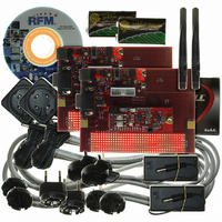
KIT DEV FOR TRC104
Manufacturer
RFM
Type
Transceiverr
Datasheets
1.DR-TRC104-2400-DK.pdf
(33 pages)
2.DR-TRC104-2400-DK.pdf
(1 pages)
3.DR-TRC104-2400-DK.pdf
(2 pages)
Specifications of DR-TRC104-2400-DK
Frequency
2.4GHz
For Use With/related Products
TRC104
Lead Free Status / RoHS Status
Lead free / RoHS Compliant
Other names
583-1137


maximum recommended value for C
is 20 pF. The required crystal frequency tolerance for the TRC104 is
L
±30 ppm maximum including temperature and aging drift. A typical ESR for the crystal is 35 ohms, and the
maximum static capacitance is 7 pF. RFM recommends the 16 MHz XTL1021 for use with the TRC104.
3.5 On-chip Regulators
The TRC104 has on-chip regulators used to power the VCO, the digital circuitry, and for biasing of the RF port.
Power pins with a VCC designation are external power inputs to the on-chip regulators. Power pins with a VDD
designation are regulated power outputs that are filtered by external capacitors or are used to power external
TRC104 functions.
3.6 Receiver
As shown in Figure 2, the TRC104 receiver chain starts with a 2.4 GHz differential input LNA, followed by an on-
chip 2.4 GHz band-pass filter. The output of the band-pass filter drives the first mixer, which converts the RF input
to the first IF frequency. The output of the first mixer is applied to the second-conversion I and Q mixers, which
are driven by I and Q LO signals 1/8 the frequency of the first LO. The outputs of the I and Q mixers are
processed by a 5 MHz complex IF filter, which provides both band-pass filtering and Hilbert transform phasing
between the I and Q channels. The phased I and Q channels are summed, nulling the unwanted image response.
The output from the complex IF filter is applied to a limiting IF amplifier, which also generates inter-stage outputs
that drive the RSSI signal summer. The limited output from the IF amplifier drives an FSK detector. The FSK
detector output is applied to a data slicer and then a data and clock recovery circuit. The recovered data and
clock signals are processed by the TRC104 control logic according to the receiver mode of operation.
3.7 RSSI
The RSSI signal is an indication of received signal strength. A diagram of the RSSI implementation is shown in
Figure 7. Once the RSSI signal is enabled by setting the RSSIA_rfsh bit of register 0x03 to 1, the TRC104 will
begin to detect the strength of incoming signals. The RSSIA pin outputs an analog voltage corresponding to the
strength of the received signal. Once the RSSI sample is complete, the RSSIA_rfsh bit resets to 0. Any reading
of the RSSIA pin or RSSID pin should be taken after the RSSIA_rfsh bit resets to 0.
Figure 7
The analog RSSI signal is applied to an ADC to obtain a digital RSSI value, RSSID. The digital value is stored in
the RSSI_val of register 0x04. The RSSI covers two ranges of signal strength, based on the state of the RSSI_G
bit in configuration register 0x04. If RSS_G is 0, the RSSI covers the received signal strength range of -95 to
www.RFM.com
E-mail:
info@rfm.com
Technical support +1.800.704.6079
Page 11 of 33
©2009 by RF Monolithics, Inc.
TRC104 - 08/13/09
Related parts for DR-TRC104-2400-DK
Image
Part Number
Description
Manufacturer
Datasheet
Request
R

Part Number:
Description:
ASH RX 115.2 KBPS 433.92 MHZ
Manufacturer:
RFM
Datasheet:

Part Number:
Description:
RFIC TRANCEIVER MULTI-CHANNEL FS
Manufacturer:
RFM
Datasheet:

Part Number:
Description:
ASH TX 115.2 KBPS 433.92 MHZ
Manufacturer:
RFM
Datasheet:
Part Number:
Description:
Filters 1602MHz BW=61MHz
Manufacturer:
RFM
Datasheet:

Part Number:
Description:
RESONATOR, SM3030-6
Manufacturer:
RFM
Datasheet:

Part Number:
Description:
RESONATOR, SM3030-6
Manufacturer:
RFM
Datasheet:

Part Number:
Description:
RESONATOR, SM3030-6
Manufacturer:
RFM
Datasheet:

Part Number:
Description:
RESONATOR, SM5035-4
Manufacturer:
RFM
Datasheet:
Part Number:
Description:
RESONATOR 418MHZ SM5035-4
Manufacturer:
RFM
Datasheet:
Part Number:
Description:
RESONATOR 315 MHZ SMD
Manufacturer:
RFM
Datasheet:
Part Number:
Description:
WiFi / 802.11 Modules 2.4 and 5.8GHz + BT
Manufacturer:
RFM
Datasheet:

Part Number:
Description:
10-Terminal Ceramic Surface-Mount Case 7 x 5 mm Nominal Footprint
Manufacturer:
RFM [RF Monolithics, Inc]
Datasheet:
Part Number:
Description:
QUAD-BAND GSM850/GSM/DCS/PCS POWER AMP MODULE
Manufacturer:
RFM [RF Monolithics, Inc]
Datasheet:
Part Number:
Description:
402 to 405 MHz Medical Band Front-end Filter
Manufacturer:
RFM [RF Monolithics, Inc]
Datasheet: