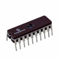
PIC16C782/JW Microchip Technology, PIC16C782/JW Datasheet - Page 76

PIC16C782/JW
Manufacturer Part Number
PIC16C782/JW
Description
IC MCU EPROM 2KX14 COMP 20CDIP
Manufacturer
Microchip Technology
Series
PIC® 16Cr
Datasheets
1.PIC16C781-ISO.pdf
(186 pages)
2.PIC16C781-ISO.pdf
(8 pages)
3.PIC16C781-ISO.pdf
(8 pages)
Specifications of PIC16C782/JW
Core Processor
PIC
Core Size
8-Bit
Speed
20MHz
Peripherals
Brown-out Detect/Reset, POR, PWM, WDT
Number Of I /o
13
Program Memory Size
3.5KB (2K x 14)
Program Memory Type
EPROM, UV
Ram Size
128 x 8
Voltage - Supply (vcc/vdd)
4 V ~ 5.5 V
Data Converters
A/D 8x8b; D/A 1x8b
Oscillator Type
Internal
Operating Temperature
0°C ~ 70°C
Package / Case
20-CDIP (0.300", 7.62mm) Window
For Use With
DVA16XP202 - ADAPTER DEVICE PIC16C781/782DM163012 - BOARD DEMO PICDEM FOR 16C781/782AC164028 - MODULE SKT PROMATEII 20SOIC/DIP
Lead Free Status / RoHS Status
Contains lead / RoHS non-compliant
Eeprom Size
-
Connectivity
-
Other names
Q1137459
Available stocks
Company
Part Number
Manufacturer
Quantity
Price
- Current page: 76 of 186
- Download datasheet (4Mb)
PIC16C781/782
FIGURE 9-2:
9.4
Example 9-2 demonstrates an ADC conversion. The
RA0/AN0 pin is configured as the analog input. The ref-
erence voltage selected is the device AV
interrupt is enabled, and the ADC conversion clock is
ADRC.
Clearing the GO/DONE bit during a conversion aborts
the current conversion. The ADRES register is NOT
updated with the partially completed ADC conversion
sample. That is, the ADRES register continues to con-
tain the value of the last completed conversion (or the
last value written to the ADRES register). After the ADC
conversion is aborted, a 2T
before the next acquisition is started. After this 2T
wait period, an acquisition is automatically started on
the selected channel.
DS41171A-page 74
ADC Configuration and
Conversion
Legend: C
VA
ANALOG INPUT MODEL
R
V
I
R
SS
C
S
LEAKAGE
T
PIN
IC
HOLD
AD
ANx
CPIN
5 pF
wait period is required
= input capacitance
= threshold voltage
= leakage current at the pin due to
= interconnect resistance
= sampling switch
= sample/hold capacitance (from DAC)
various junctions
DD
. The ADC
V
DD
V
V
T
T
Preliminary
= 0.6V
= 0.6V
AD
I
± 500 nA
LEAKAGE
EXAMPLE 9-2:
;********************************************
;*
;*
;*
;*
;*
;*
;*
;********************************************
;*
;*
;*
ADC_CNVRT
ADC_CN_LOOP
R
IC
This code block will configure the ADC
Conversion start & wait for complete
for polling, AVDD as reference, RC clock
and RA0 input.
polling code included.
minimum acquisition delay from
configuration.
BANKSEL
CLRF
BSF
BSF
BANKSEL
MOVLW
MOVWF
Start & Wait for ADC complete, assumes
BANKSEL
BSF
BTFSC
GOTO
MOVF
1k
V
SS R
DD
Sampling
Switch
6V
5V
4V
3V
2V
SS
ADCON1
ADCON1
TRISA,0
ANSEL,0
ADCON0
B’11000001’
ADCON0
ADCON0
ADCON0,GO
ADCON0,GO
ADC_CN_LOOP ; If not, wait
ADRES,W
Sampling Switch
5 6 7 8 9 10 11
ADC CONVERSION
V
SS
C
= DAC capacitance
= 51.2 pF
( k
HOLD
2001 Microchip Technology Inc.
)
; Select Bank 1
; AVDD as VREF
; Set RA0 as input
; Set RA0 as analog
; Select Bank0
; RC, Ch 0, ADC on
; Select Bank 0
; Start convert
; Test for end
; Get result
Related parts for PIC16C782/JW
Image
Part Number
Description
Manufacturer
Datasheet
Request
R

Part Number:
Description:
3.5KB Flash, 128B RAM, 18 I/O, CLC, CWG, DDS, 10-bit ADC 20 QFN 4x4mm TUBE
Manufacturer:
Microchip Technology
Datasheet:

Part Number:
Description:
3.5KB Flash, 128B RAM, 18 I/O, CLC, CWG, DDS, 10-bit ADC 20 PDIP .300in TUBE
Manufacturer:
Microchip Technology
Datasheet:

Part Number:
Description:
3.5KB Flash, 128B RAM, 18 I/O, CLC, CWG, DDS, 10-bit ADC 20 SOIC .300in TUBE
Manufacturer:
Microchip Technology
Datasheet:

Part Number:
Description:
3.5KB Flash, 128B RAM, 18 I/O, CLC, CWG, DDS, 10-bit ADC 20 SSOP .209in TUBE
Manufacturer:
Microchip Technology
Datasheet:

Part Number:
Description:
3.5KB Flash, 128B RAM, 18 I/O, CLC, CWG, DDS, 10-bit ADC 20 QFN 4x4mm TUBE
Manufacturer:
Microchip Technology
Datasheet:

Part Number:
Description:
3.5KB Flash, 128B RAM, 18 I/O, CLC, CWG, DDS, 10-bit ADC 20 PDIP .300in TUBE
Manufacturer:
Microchip Technology
Datasheet:

Part Number:
Description:
3.5KB Flash, 128B RAM, 18 I/O, CLC, CWG, DDS, 10-bit ADC 20 SOIC .300in TUBE
Manufacturer:
Microchip Technology
Datasheet:

Part Number:
Description:
3.5KB Flash, 128B RAM, 18 I/O, CLC, CWG, DDS, 10-bit ADC 20 SSOP .209in TUBE
Manufacturer:
Microchip Technology
Datasheet:

Part Number:
Description:
3.5KB Flash, 128B RAM, 18 I/O, CLC, CWG, DDS, 10-bit ADC 20 QFN 4x4mm T/R
Manufacturer:
Microchip Technology
Datasheet:

Part Number:
Description:
3.5KB Flash, 128B RAM, 18 I/O, CLC, CWG, DDS, 10-bit ADC 20 SOIC .300in T/R
Manufacturer:
Microchip Technology
Datasheet:

Part Number:
Description:
3.5KB Flash, 128B RAM, 18 I/O, CLC, CWG, DDS, 10-bit ADC 20 SSOP .209in T/R
Manufacturer:
Microchip Technology
Datasheet:

Part Number:
Description:
3.5KB Flash, 128B RAM, 18 I/O, CLC, CWG, DDS, 10-bit ADC 20 QFN 4x4mm TUBE
Manufacturer:
Microchip Technology
Datasheet:

Part Number:
Description:
3.5KB Flash, 128B RAM, 18 I/O, CLC, CWG, DDS, 10-bit ADC 20 PDIP .300in TUBE
Manufacturer:
Microchip Technology
Datasheet:

Part Number:
Description:
3.5KB Flash, 128B RAM, 18 I/O, CLC, CWG, DDS, 10-bit ADC 20 SOIC .300in TUBE
Manufacturer:
Microchip Technology
Datasheet:

Part Number:
Description:
3.5KB Flash, 128B RAM, 18 I/O, CLC, CWG, DDS, 10-bit ADC 20 SSOP .209in TUBE
Manufacturer:
Microchip Technology
Datasheet:


