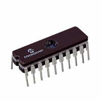
PIC16C782/JW Microchip Technology, PIC16C782/JW Datasheet - Page 109

PIC16C782/JW
Manufacturer Part Number
PIC16C782/JW
Description
IC MCU EPROM 2KX14 COMP 20CDIP
Manufacturer
Microchip Technology
Series
PIC® 16Cr
Datasheets
1.PIC16C781-ISO.pdf
(186 pages)
2.PIC16C781-ISO.pdf
(8 pages)
3.PIC16C781-ISO.pdf
(8 pages)
Specifications of PIC16C782/JW
Core Processor
PIC
Core Size
8-Bit
Speed
20MHz
Peripherals
Brown-out Detect/Reset, POR, PWM, WDT
Number Of I /o
13
Program Memory Size
3.5KB (2K x 14)
Program Memory Type
EPROM, UV
Ram Size
128 x 8
Voltage - Supply (vcc/vdd)
4 V ~ 5.5 V
Data Converters
A/D 8x8b; D/A 1x8b
Oscillator Type
Internal
Operating Temperature
0°C ~ 70°C
Package / Case
20-CDIP (0.300", 7.62mm) Window
For Use With
DVA16XP202 - ADAPTER DEVICE PIC16C781/782DM163012 - BOARD DEMO PICDEM FOR 16C781/782AC164028 - MODULE SKT PROMATEII 20SOIC/DIP
Lead Free Status / RoHS Status
Contains lead / RoHS non-compliant
Eeprom Size
-
Connectivity
-
Other names
Q1137459
Available stocks
Company
Part Number
Manufacturer
Quantity
Price
- Current page: 109 of 186
- Download datasheet (4Mb)
13.3
The programmable nature of the PSMC lends itself to a
wide variety of applications involving current or voltage
management. The following examples are intended to
provide suggested applications for the PSMC. The
examples are not complete designs, but rather block
diagrams of some potential applications of the PSMC.
For a broader list of applications, including supporting
math and firmware examples, please refer to Microchip
web page for applicable Application Notes.
13.3.1
In this example, the PSMC controls the boost configu-
ration switching power supply in Figure 13-5.
The PSMC is configured as a two feedback loop PWM,
current mode, switching power supply controller. The
inner current feedback loops consist of:
• PSMC
• MOSFET driver
• Power MOSFET Q1
• Inductor L1
• Current transformer
• Comparator C1
The outer voltage feedback loop consists of:
• Diode D1
• C
• OPAMP feedback filter
• DAC reference
2001 Microchip Technology Inc.
MAIN
Configuration
EXAMPLE BOOST LC SWITCHING
POWER SUPPLY
Preliminary
The inner current loop is a pulsed current source driven
by the PSMC. During the active phase of the output
pulse, the inner loop builds up a current flow in inductor
L1. The current in L1 is monitored by the current trans-
former. The output of the transformer is offset by the
ramp from the slope compensation network R3/C1 and
then fed into the comparator. When the voltage (pro-
portional to the current flow in L1, offset by the slope
compensation) exceeds the error voltage from the
OPAMP, Q1 is turned off and L1 discharges through D1
into C
The outer voltage loop monitors the output voltage
across C
the DAC is subtracted, generating the raw error volt-
age. The raw error voltage is filtered by the OPAMP
and routed to Comparator C1 in the inner current loop.
The phase compensation output of the PSMC acts to
improve loop stability by adding a pseudo-ramp wave-
form to the current sense transformer feedback in the
inner loop. In conditions where the charge phase of the
cycle is greater then 50%, the increased current feed-
back reduces the current charge in L1, slowing the
charging of C
all loop gain for duty cycles of >50%, maintaining loop
stability.
MAIN
MAIN
for the remainder of the period.
MAIN
using R1/R2. The reference voltage from
PIC16C781/782
. The result is a reduction in the over-
DS41171A-page 107
Related parts for PIC16C782/JW
Image
Part Number
Description
Manufacturer
Datasheet
Request
R

Part Number:
Description:
3.5KB Flash, 128B RAM, 18 I/O, CLC, CWG, DDS, 10-bit ADC 20 QFN 4x4mm TUBE
Manufacturer:
Microchip Technology
Datasheet:

Part Number:
Description:
3.5KB Flash, 128B RAM, 18 I/O, CLC, CWG, DDS, 10-bit ADC 20 PDIP .300in TUBE
Manufacturer:
Microchip Technology
Datasheet:

Part Number:
Description:
3.5KB Flash, 128B RAM, 18 I/O, CLC, CWG, DDS, 10-bit ADC 20 SOIC .300in TUBE
Manufacturer:
Microchip Technology
Datasheet:

Part Number:
Description:
3.5KB Flash, 128B RAM, 18 I/O, CLC, CWG, DDS, 10-bit ADC 20 SSOP .209in TUBE
Manufacturer:
Microchip Technology
Datasheet:

Part Number:
Description:
3.5KB Flash, 128B RAM, 18 I/O, CLC, CWG, DDS, 10-bit ADC 20 QFN 4x4mm TUBE
Manufacturer:
Microchip Technology
Datasheet:

Part Number:
Description:
3.5KB Flash, 128B RAM, 18 I/O, CLC, CWG, DDS, 10-bit ADC 20 PDIP .300in TUBE
Manufacturer:
Microchip Technology
Datasheet:

Part Number:
Description:
3.5KB Flash, 128B RAM, 18 I/O, CLC, CWG, DDS, 10-bit ADC 20 SOIC .300in TUBE
Manufacturer:
Microchip Technology
Datasheet:

Part Number:
Description:
3.5KB Flash, 128B RAM, 18 I/O, CLC, CWG, DDS, 10-bit ADC 20 SSOP .209in TUBE
Manufacturer:
Microchip Technology
Datasheet:

Part Number:
Description:
3.5KB Flash, 128B RAM, 18 I/O, CLC, CWG, DDS, 10-bit ADC 20 QFN 4x4mm T/R
Manufacturer:
Microchip Technology
Datasheet:

Part Number:
Description:
3.5KB Flash, 128B RAM, 18 I/O, CLC, CWG, DDS, 10-bit ADC 20 SOIC .300in T/R
Manufacturer:
Microchip Technology
Datasheet:

Part Number:
Description:
3.5KB Flash, 128B RAM, 18 I/O, CLC, CWG, DDS, 10-bit ADC 20 SSOP .209in T/R
Manufacturer:
Microchip Technology
Datasheet:

Part Number:
Description:
3.5KB Flash, 128B RAM, 18 I/O, CLC, CWG, DDS, 10-bit ADC 20 QFN 4x4mm TUBE
Manufacturer:
Microchip Technology
Datasheet:

Part Number:
Description:
3.5KB Flash, 128B RAM, 18 I/O, CLC, CWG, DDS, 10-bit ADC 20 PDIP .300in TUBE
Manufacturer:
Microchip Technology
Datasheet:

Part Number:
Description:
3.5KB Flash, 128B RAM, 18 I/O, CLC, CWG, DDS, 10-bit ADC 20 SOIC .300in TUBE
Manufacturer:
Microchip Technology
Datasheet:

Part Number:
Description:
3.5KB Flash, 128B RAM, 18 I/O, CLC, CWG, DDS, 10-bit ADC 20 SSOP .209in TUBE
Manufacturer:
Microchip Technology
Datasheet:


