PIC16C782/JW Microchip Technology, PIC16C782/JW Datasheet - Page 53
PIC16C782/JW
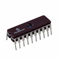
Manufacturer Part Number
PIC16C782/JW
Description
IC MCU EPROM 2KX14 COMP 20CDIP
Manufacturer
Microchip Technology
Series
PIC® 16Cr
Datasheets
1.PIC16C781-ISO.pdf
(186 pages)
2.PIC16C781-ISO.pdf
(8 pages)
3.PIC16C781-ISO.pdf
(8 pages)
Specifications of PIC16C782/JW
Core Processor
PIC
Core Size
8-Bit
Speed
20MHz
Peripherals
Brown-out Detect/Reset, POR, PWM, WDT
Number Of I /o
13
Program Memory Size
3.5KB (2K x 14)
Program Memory Type
EPROM, UV
Ram Size
128 x 8
Voltage - Supply (vcc/vdd)
4 V ~ 5.5 V
Data Converters
A/D 8x8b; D/A 1x8b
Oscillator Type
Internal
Operating Temperature
0°C ~ 70°C
Package / Case
20-CDIP (0.300", 7.62mm) Window
For Use With
DVA16XP202 - ADAPTER DEVICE PIC16C781/782DM163012 - BOARD DEMO PICDEM FOR 16C781/782AC164028 - MODULE SKT PROMATEII 20SOIC/DIP
Lead Free Status / RoHS Status
Contains lead / RoHS non-compliant
Eeprom Size
-
Connectivity
-
Other names
Q1137459
Available stocks
Company
Part Number
Manufacturer
Quantity
Price


5.0
The Timer0 module timer/counter has the following
features:
• 8-bit timer/counter
• Readable and writable
• Internal or external clock select
• Edge select for external clock
• 8-bit software programmable prescaler
• Interrupt on overflow from FFh to 00h
Figure 5-1 is a simplified block diagram of the Timer0
module.
Additional information on timer modules is available in
the
(DS33023).
5.1
Timer0 can operate as either a timer or a counter.
Programming Timer0 is via the OPTION register (see
Register 2-2).
Timer0 mode is selected by clearing/setting the bit
T0CS (OPTION_REG<5>). In Timer mode (T0CS = 0),
the Timer0 module increments every instruction cycle
(without prescaler). If the TMR0 register is written, the
increment is inhibited for the following two instruction
cycles. The user can work around this by writing an
adjusted value to the TMR0 register.
Counter mode is selected by setting bit T0CS
(OPTION_REG<5>).
increments either on every rising, or falling edge of pin
RA4/T0CKI. The incrementing edge is determined by
the
(OPTION_REG<4>). Clearing bit T0SE selects the ris-
ing edge, setting selects the falling edge. Restrictions
on the external clock input are discussed below.
FIGURE 5-1:
2001 Microchip Technology Inc.
RA4/T0CKI
pin
Note 1: T0CS, T0SE, PSA, PS<2:0> (OPTION_REG<5:0>).
PICmicro™
Timer0
TIMER0 MODULE
Timer0 Operation
2: The prescaler is shared with Watchdog Timer (refer to Figure 5-2 for detailed block diagram).
T0SE
Source
F
OSC
Mid-Range
TIMER0 BLOCK DIAGRAM
/4
In
Edge
Counter
T0CS
Reference
0
1
Select
mode,
Programmable
bit
PS<2:0>
Prescaler
Manual,
Timer0
T0SE
3
Preliminary
PSA
1
0
PSOUT
When an external clock input is used for Timer0, it must
meet certain requirements. The requirements ensure
the external clock can be synchronized with the internal
system clock. Also, there is a delay in the actual incre-
menting of Timer0 after synchronization.
Additional information on external clock requirements
is available in the PICmicro™ Mid-Range Reference
Manual, (DS33023).
EXAMPLE 5-1:
;* This code block will configure Timer0
;* for Polling, internal clock & 1:16
;*
;*
;* Wait for TMR0 overflow code included
********************************************
;*
;*
T0_OVFL_WAIT
prescaler
BANKSEL
CLRF
BANKSEL
MOVLW
MOVWF
Wait for TMR0 overflow
TBFSS
GOTO
BCF
(2 T
Sync with
Internal
Clocks
CY
Delay)
PIC16C781/782
TMR0
TMR0
OPTION_REG
B’11000011’
OPTION_REG
INTCON,T0IF
T0_OVFL_WAIT ; If clear, test
INTCON,T0IF
PSOUT
INITIALIZING TIMER0
Data Bus
TMR0
; Select Bank 0
; Clear Timer0
; Register
; Select Bank 1
; INT on L2H
; Internal clk,
; pscaler 1:16
; Check for TMR0
; overflow
; again
; Clear interrupt
8
DS41171A-page 51
Flag bit T0IF
Set Interrupt
on Overflow
Related parts for PIC16C782/JW
Image
Part Number
Description
Manufacturer
Datasheet
Request
R

Part Number:
Description:
3.5KB Flash, 128B RAM, 18 I/O, CLC, CWG, DDS, 10-bit ADC 20 QFN 4x4mm TUBE
Manufacturer:
Microchip Technology
Datasheet:

Part Number:
Description:
3.5KB Flash, 128B RAM, 18 I/O, CLC, CWG, DDS, 10-bit ADC 20 PDIP .300in TUBE
Manufacturer:
Microchip Technology
Datasheet:

Part Number:
Description:
3.5KB Flash, 128B RAM, 18 I/O, CLC, CWG, DDS, 10-bit ADC 20 SOIC .300in TUBE
Manufacturer:
Microchip Technology
Datasheet:

Part Number:
Description:
3.5KB Flash, 128B RAM, 18 I/O, CLC, CWG, DDS, 10-bit ADC 20 SSOP .209in TUBE
Manufacturer:
Microchip Technology
Datasheet:
Part Number:
Description:
3.5KB Flash, 128B RAM, 18 I/O, CLC, CWG, DDS, 10-bit ADC 20 QFN 4x4mm TUBE
Manufacturer:
Microchip Technology
Datasheet:
Part Number:
Description:
3.5KB Flash, 128B RAM, 18 I/O, CLC, CWG, DDS, 10-bit ADC 20 PDIP .300in TUBE
Manufacturer:
Microchip Technology
Datasheet:
Part Number:
Description:
3.5KB Flash, 128B RAM, 18 I/O, CLC, CWG, DDS, 10-bit ADC 20 SOIC .300in TUBE
Manufacturer:
Microchip Technology
Datasheet:
Part Number:
Description:
3.5KB Flash, 128B RAM, 18 I/O, CLC, CWG, DDS, 10-bit ADC 20 SSOP .209in TUBE
Manufacturer:
Microchip Technology
Datasheet:
Part Number:
Description:
3.5KB Flash, 128B RAM, 18 I/O, CLC, CWG, DDS, 10-bit ADC 20 QFN 4x4mm T/R
Manufacturer:
Microchip Technology
Datasheet:
Part Number:
Description:
3.5KB Flash, 128B RAM, 18 I/O, CLC, CWG, DDS, 10-bit ADC 20 SOIC .300in T/R
Manufacturer:
Microchip Technology
Datasheet:
Part Number:
Description:
3.5KB Flash, 128B RAM, 18 I/O, CLC, CWG, DDS, 10-bit ADC 20 SSOP .209in T/R
Manufacturer:
Microchip Technology
Datasheet:
Part Number:
Description:
3.5KB Flash, 128B RAM, 18 I/O, CLC, CWG, DDS, 10-bit ADC 20 QFN 4x4mm TUBE
Manufacturer:
Microchip Technology
Datasheet:
Part Number:
Description:
3.5KB Flash, 128B RAM, 18 I/O, CLC, CWG, DDS, 10-bit ADC 20 PDIP .300in TUBE
Manufacturer:
Microchip Technology
Datasheet:
Part Number:
Description:
3.5KB Flash, 128B RAM, 18 I/O, CLC, CWG, DDS, 10-bit ADC 20 SOIC .300in TUBE
Manufacturer:
Microchip Technology
Datasheet:
Part Number:
Description:
3.5KB Flash, 128B RAM, 18 I/O, CLC, CWG, DDS, 10-bit ADC 20 SSOP .209in TUBE
Manufacturer:
Microchip Technology
Datasheet: