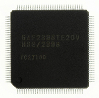
HD64F2145BTE20 Renesas Electronics America, HD64F2145BTE20 Datasheet - Page 42

HD64F2145BTE20
Manufacturer Part Number
HD64F2145BTE20
Description
IC H8S MCU FLASH 256K 100-QFP
Manufacturer
Renesas Electronics America
Series
H8® H8S/2100r
Specifications of HD64F2145BTE20
Core Processor
H8S/2000
Core Size
16-Bit
Speed
20MHz
Connectivity
I²C, IrDA, SCI, X-Bus
Peripherals
PWM, WDT
Number Of I /o
74
Program Memory Size
256KB (256K x 8)
Program Memory Type
FLASH
Ram Size
8K x 8
Voltage - Supply (vcc/vdd)
4.5 V ~ 5.5 V
Data Converters
A/D 8x10b; D/A 2x8b
Oscillator Type
Internal
Operating Temperature
-20°C ~ 75°C
Package / Case
100-TQFP, 100-VQFP
Lead Free Status / RoHS Status
Contains lead / RoHS non-compliant
Eeprom Size
-
- Current page: 42 of 847
- Download datasheet (5Mb)
Figure 7.4
Figure 7.5
Figure 7.6
Figure 7.7
Figure 7.8
Figure 7.9
Figure 7.10
Figure 7.11
Section 9 8-Bit PWM Timer (PWM)
Figure 9.1
Figure 9.2
Section 10 14-Bit PWM Timer (PWMX)
Figure 10.1
Figure 10.2
Figure 10.3
Figure 10.4
Figure 10.5
Figure 10.6
Section 11 16-Bit Free-Running Timer (FRT)
Figure 11.1
Figure 11.2
Figure 11.3
Figure 11.4
Figure 11.5
Figure 11.6
Figure 11.7
Figure 11.8
Figure 11.9
Figure 11.10 Buffered Input Capture Timing (BUFEA = 1)..................................................... 275
Figure 11.11 Timing of Input Capture Flag (ICFA, ICFB, ICFC, or ICFD) Setting ................ 276
Figure 11.12 Timing of Output Compare Flag (OCFA or OCFB) Setting................................ 277
Figure 11.13 Timing of Overflow Flag (OVF) Setting ............................................................. 277
Figure 11.14 OCRA Automatic Addition Timing..................................................................... 278
Figure 11.15 Timing of Input Capture Mask Signal Setting ..................................................... 278
Figure 11.16 Timing of Input Capture Mask Signal Clearing................................................... 279
Figure 11.17 FRC Write-Clear Conflict.................................................................................... 280
Figure 11.18 FRC Write-Increment Conflict ............................................................................ 281
Rev. 3.00 Mar 21, 2006 page xl of liv
DTC Operation Flowchart ................................................................................... 155
Memory Mapping in Normal Mode..................................................................... 156
Memory Mapping in Repeat Mode...................................................................... 157
Memory Mapping in Block Transfer Mode ......................................................... 158
Chain Transfer Operation .................................................................................... 159
DTC Operation Timing (Example in Normal Mode or Repeat Mode) ................ 160
DTC Operation Timing (Example of Block Transfer Mode,
with Block Size of 2) ........................................................................................... 161
DTC Operation Timing (Example of Chain Transfer)......................................... 161
Block Diagram of PWM Timer ........................................................................... 232
Example of Additional Pulse Timing (when Upper 4 Bits of PWDR = 1000) .... 240
PWM (D/A) Block Diagram ................................................................................ 243
PWM D/A Operation ........................................................................................... 251
Output Waveform (OS = 0, DADR Corresponds to T
Output Waveform (OS = 1, DADR Corresponds to T
D/A Data Register Configuration when CFS = 1................................................. 254
Output Waveform when DADR = H'0207 (OS = 1)............................................ 255
Block Diagram of 16-Bit Free-Running Timer.................................................... 260
Example of Pulse Output ..................................................................................... 271
Increment Timing with Internal Clock Source..................................................... 272
Increment Timing with External Clock Source ................................................... 272
Timing of Output Compare A Output.................................................................. 273
Clearing of FRC by Compare-Match A Signal.................................................... 273
Input Capture Input Signal Timing (Usual Case)................................................. 274
Input Capture Input Signal Timing (When ICRA to ICRD are Read) ................. 274
Buffered Input Capture Timing............................................................................ 275
L
H
) ...................................... 253
) ...................................... 254
Related parts for HD64F2145BTE20
Image
Part Number
Description
Manufacturer
Datasheet
Request
R

Part Number:
Description:
KIT STARTER FOR M16C/29
Manufacturer:
Renesas Electronics America
Datasheet:

Part Number:
Description:
KIT STARTER FOR R8C/2D
Manufacturer:
Renesas Electronics America
Datasheet:

Part Number:
Description:
R0K33062P STARTER KIT
Manufacturer:
Renesas Electronics America
Datasheet:

Part Number:
Description:
KIT STARTER FOR R8C/23 E8A
Manufacturer:
Renesas Electronics America
Datasheet:

Part Number:
Description:
KIT STARTER FOR R8C/25
Manufacturer:
Renesas Electronics America
Datasheet:

Part Number:
Description:
KIT STARTER H8S2456 SHARPE DSPLY
Manufacturer:
Renesas Electronics America
Datasheet:

Part Number:
Description:
KIT STARTER FOR R8C38C
Manufacturer:
Renesas Electronics America
Datasheet:

Part Number:
Description:
KIT STARTER FOR R8C35C
Manufacturer:
Renesas Electronics America
Datasheet:

Part Number:
Description:
KIT STARTER FOR R8CL3AC+LCD APPS
Manufacturer:
Renesas Electronics America
Datasheet:

Part Number:
Description:
KIT STARTER FOR RX610
Manufacturer:
Renesas Electronics America
Datasheet:

Part Number:
Description:
KIT STARTER FOR R32C/118
Manufacturer:
Renesas Electronics America
Datasheet:

Part Number:
Description:
KIT DEV RSK-R8C/26-29
Manufacturer:
Renesas Electronics America
Datasheet:

Part Number:
Description:
KIT STARTER FOR SH7124
Manufacturer:
Renesas Electronics America
Datasheet:

Part Number:
Description:
KIT STARTER FOR H8SX/1622
Manufacturer:
Renesas Electronics America
Datasheet:

Part Number:
Description:
KIT DEV FOR SH7203
Manufacturer:
Renesas Electronics America
Datasheet:


