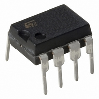
ST7FLITEUS5B6 STMicroelectronics, ST7FLITEUS5B6 Datasheet - Page 38

ST7FLITEUS5B6
Manufacturer Part Number
ST7FLITEUS5B6
Description
MCU 8BIT 1KB FLASH 128KB 8-DIP
Manufacturer
STMicroelectronics
Series
ST7r
Datasheet
1.STEVAL-IFS006V1.pdf
(136 pages)
Specifications of ST7FLITEUS5B6
Core Processor
ST7
Core Size
8-Bit
Speed
8MHz
Peripherals
LVD, POR, PWM, WDT
Number Of I /o
5
Program Memory Size
1KB (1K x 8)
Program Memory Type
FLASH
Ram Size
128 x 8
Voltage - Supply (vcc/vdd)
2.4 V ~ 5.5 V
Data Converters
A/D 5x10b
Oscillator Type
Internal
Operating Temperature
-40°C ~ 85°C
Package / Case
8-DIP (0.300", 7.62mm)
Controller Family/series
ST7
No. Of I/o's
5
Ram Memory Size
128Byte
Cpu Speed
8MHz
No. Of Timers
2
Rohs Compliant
Yes
For Use With
497-6403 - BOARD EVAL 8BIT MICRO + TDE1708497-6407 - BOARD EVAL FOR VACUUM CLEANER497-5861 - EVAL BRD POWER MOSFET/8PIN MCU497-5858 - EVAL BOARD PLAYBACK ST7FLITE497-5515 - EVAL BOARD PHASE CTRL DIMMER497-5049 - KIT STARTER RAISONANCE ST7FLITE497-5046 - KIT TOOL FOR ST7/UPSD/STR7 MCU
Lead Free Status / RoHS Status
Lead free / RoHS Compliant
Eeprom Size
-
Connectivity
-
Other names
497-5636-5
Available stocks
Company
Part Number
Manufacturer
Quantity
Price
Company:
Part Number:
ST7FLITEUS5B6
Manufacturer:
STMicroelectronics
Quantity:
8
Supply, reset and clock management
38/136
This 16-bit register is read/write by software but can be written only once between two reset
events. It is cleared by hardware after a reset; When both MUXCR0 and MUXCR1 registers
are at 00h, the multiplexed PA3/RESET pin will act as RESET. To configure this pin as
output (Port A3), write 55h to MUXCR0 and AAh to MUXCR1.
These registers are one-time writable only.
●
●
Table 8.
0047h
0048h
Address
(Hex.)
To configure PA3 as general purpose output:
After power-on / reset, the application program has to configure the I/O port by writing
to these registers as described above. Once the pin is configured as an I/O output, it
cannot be changed back to a reset pin by the application code.
To configure PA3 as RESET:
An internally generated reset (such as POR, LVD, WDG, illegal opcode) will clear the
two registers and the pin will act again as a reset function. Otherwise, a power-down is
required to put the pin back in reset configuration.
MUXCR0
reset
value
MUXCR1
reset
value
Register
Multiplexed IO register map and reset values
label
MIR15
MIR7
7
0
0
MIR14
MIR6
6
0
0
MIR13
MIR5
5
0
0
MIR12
MIR4
4
0
0
MIR11
MIR3
3
0
0
ST7LITEUS2, ST7LITEUS5
MIR10
MIR2
2
0
0
MIR1
MIR9
1
0
0
MIR0
MIR8
0
0
0


