ST7FLITEUS5B6 STMicroelectronics, ST7FLITEUS5B6 Datasheet - Page 124

ST7FLITEUS5B6
Manufacturer Part Number
ST7FLITEUS5B6
Description
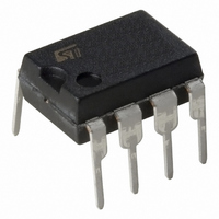
MCU 8BIT 1KB FLASH 128KB 8-DIP
Manufacturer
STMicroelectronics
Series
ST7r
Datasheet
1.STEVAL-IFS006V1.pdf
(136 pages)
Specifications of ST7FLITEUS5B6
Core Processor
ST7
Core Size
8-Bit
Speed
8MHz
Peripherals
LVD, POR, PWM, WDT
Number Of I /o
5
Program Memory Size
1KB (1K x 8)
Program Memory Type
FLASH
Ram Size
128 x 8
Voltage - Supply (vcc/vdd)
2.4 V ~ 5.5 V
Data Converters
A/D 5x10b
Oscillator Type
Internal
Operating Temperature
-40°C ~ 85°C
Package / Case
8-DIP (0.300", 7.62mm)
Controller Family/series
ST7
No. Of I/o's
5
Ram Memory Size
128Byte
Cpu Speed
8MHz
No. Of Timers
2
Rohs Compliant
Yes
For Use With
497-6403 - BOARD EVAL 8BIT MICRO + TDE1708497-6407 - BOARD EVAL FOR VACUUM CLEANER497-5861 - EVAL BRD POWER MOSFET/8PIN MCU497-5858 - EVAL BOARD PLAYBACK ST7FLITE497-5515 - EVAL BOARD PHASE CTRL DIMMER497-5049 - KIT STARTER RAISONANCE ST7FLITE497-5046 - KIT TOOL FOR ST7/UPSD/STR7 MCU
Lead Free Status / RoHS Status
Lead free / RoHS Compliant
Eeprom Size
-
Connectivity
-
Other names
497-5636-5
Available stocks
Company
Part Number
Manufacturer
Quantity
Price
Company:
Part Number:
ST7FLITEUS5B6
Manufacturer:
STMicroelectronics
Quantity:
8
Device configuration and ordering information
14.1.2
124/136
Table 75.
Table 76.
OPTION BYTE 0
Table 77.
Internal RC as Startup Clock
Reserved
AWU RC as a Startup Clock
Reserved
External Clock on pin PA5
LVD Off
Highest voltage threshold
Medium voltage threshold
Lowest voltage threshold
Bits 7:4 Reserved, must always be 1.
Bit 3 Reserved, must always be 0.
Bit 2 SEC0 Sector 0 size definition
Bit 1 FMP_R Readout protection
Bit 0 FMP_W FLASH write protection
Startup clock selection
LVD threshold configuration
Definition of sector 0 size
Sector 0 Size
This option bit indicates the size of sector 0 according to the following table (see
Table 77: Definition of sector 0
Readout protection, when selected provides a protection against program memory
content extraction and against write access to Flash memory. Erasing the option
bytes when the FMP_R option is selected will cause the whole memory to be
erased first, and the device can be reprogrammed. Refer to
ST7 Flash Programming Reference Manual for more details.
0: Readout protection off
1: Readout protection on
This option indicates if the FLASH program memory is write protected.
Warning: When this option is selected, the program memory (and the option bit
itself) can never be erased or programmed again.
0: Write protection off
1: Write protection on
0.5k
1k
Configuration
Configuration
size).
CKSEL1
SEC0
ST7LITEUS2, ST7LITEUS5
0
1
0
0
0
1
1
Section 4.5
LVD1
1
1
0
0
CKSEL0
and the
0
0
1
0
1
LVD0
1
0
1
0


