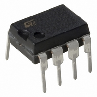
ST7FLITEUS5B6 STMicroelectronics, ST7FLITEUS5B6 Datasheet - Page 113

ST7FLITEUS5B6
Manufacturer Part Number
ST7FLITEUS5B6
Description
MCU 8BIT 1KB FLASH 128KB 8-DIP
Manufacturer
STMicroelectronics
Series
ST7r
Datasheet
1.STEVAL-IFS006V1.pdf
(136 pages)
Specifications of ST7FLITEUS5B6
Core Processor
ST7
Core Size
8-Bit
Speed
8MHz
Peripherals
LVD, POR, PWM, WDT
Number Of I /o
5
Program Memory Size
1KB (1K x 8)
Program Memory Type
FLASH
Ram Size
128 x 8
Voltage - Supply (vcc/vdd)
2.4 V ~ 5.5 V
Data Converters
A/D 5x10b
Oscillator Type
Internal
Operating Temperature
-40°C ~ 85°C
Package / Case
8-DIP (0.300", 7.62mm)
Controller Family/series
ST7
No. Of I/o's
5
Ram Memory Size
128Byte
Cpu Speed
8MHz
No. Of Timers
2
Rohs Compliant
Yes
For Use With
497-6403 - BOARD EVAL 8BIT MICRO + TDE1708497-6407 - BOARD EVAL FOR VACUUM CLEANER497-5861 - EVAL BRD POWER MOSFET/8PIN MCU497-5858 - EVAL BOARD PLAYBACK ST7FLITE497-5515 - EVAL BOARD PHASE CTRL DIMMER497-5049 - KIT STARTER RAISONANCE ST7FLITE497-5046 - KIT TOOL FOR ST7/UPSD/STR7 MCU
Lead Free Status / RoHS Status
Lead free / RoHS Compliant
Eeprom Size
-
Connectivity
-
Other names
497-5636-5
Available stocks
Company
Part Number
Manufacturer
Quantity
Price
Company:
Part Number:
ST7FLITEUS5B6
Manufacturer:
STMicroelectronics
Quantity:
8
ST7LITEUS2, ST7LITEUS5
12.9
Figure 59. Typical V
Figure 60. Typical V
Control pin characteristics
The reset network protects the device against parasitic resets.
The output of the external reset circuit must have an open-drain output to drive the ST7
reset pad. Otherwise the device can be damaged when the ST7 generates an internal reset
(LVD or watchdog).
Whatever the reset source is (internal or external), the user must ensure that the level on the
RESET pin can go below the V
not be taken into account internally.
Because the reset circuit is designed to allow the internal reset to be output in the RESET
pin, the user must ensure that the current sunk on the RESET pin is less than the absolute
maximum value specified for I
Refer to
LVD enabled and disabled.
100
90
80
70
60
50
40
200
180
160
140
120
100
80
60
40
2.4 2.6 2.8
2.4 2.6 2.8
Figure 61
3
3
3.2 3.4 3.6 3.8
3.2 3.4 3.6 3.8
and
4
4
Vdd [V]
OL
DD
Vdd [V]
4.2 4.4 4.6 4.8
Figure 62
4.2 4.4 4.6 4.8
900
800
700
600
500
400
300
200
-V
vs. V
2.4 2.6 2.8
OH
INJ(RESET)
vs. V
DD
IL
5
5
5.2 5.4 5.6 5.8
max. level specified in
for a description of the RESET pin protection circuit with
3
5.2 5.4 5.6 5.8
(HS pins)
3.2 3.4 3.6 3.8
DD
-45°C
25°C
90°C
130°C
-45°C
25°C
90°C
130°C
(HS pins)
in
6
6
Table
4
Vdd [V]
4.2 4.4 4.6 4.8
500
450
400
350
300
250
200
150
100
700
600
500
400
300
200
100
44.
2.4 2.6
2.4 2.6
2.8
2.8
5
Table
3
3
5.2 5.4 5.6 5.8
3.2 3.4 3.6
3.2 3.4
65. Otherwise the reset will
-45°C
25°C
90°C
130°C
3.6 3.8
3.8
Electrical characteristics
6
4
4
Vdd [V]
Vdd [V]
4.2 4.4 4.6
4.2 4.4 4.6 4.8
4.8
5
5
5.2 5.4 5.6
5.2 5.4 5.6
-45°C
25°C
90°C
130°C
-45°C
25°C
90°C
130°C
113/136
5.8
5.8
6
6


