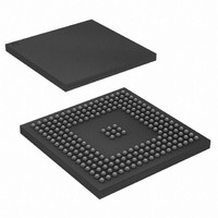
AT91SAM9XE256-CU Atmel, AT91SAM9XE256-CU Datasheet - Page 66

AT91SAM9XE256-CU
Manufacturer Part Number
AT91SAM9XE256-CU
Description
MCU ARM9 256K FLASH 217-BGA
Manufacturer
Atmel
Series
AT91SAMr
Specifications of AT91SAM9XE256-CU
Core Processor
ARM9
Core Size
16/32-Bit
Speed
180MHz
Connectivity
EBI/EMI, Ethernet, I²C, MMC, SPI, SSC, UART/USART, USB
Peripherals
Brown-out Detect/Reset, POR, PWM, WDT
Number Of I /o
96
Program Memory Size
256KB (256K x 8)
Program Memory Type
FLASH
Ram Size
56K x 8
Voltage - Supply (vcc/vdd)
1.65 V ~ 1.95 V
Data Converters
A/D 4x10b
Oscillator Type
Internal
Operating Temperature
-40°C ~ 85°C
Package / Case
217-LFBGA
Processor Series
AT91SAMx
Core
ARM926EJ-S
Data Bus Width
32 bit
Data Ram Size
32 KB
Interface Type
2-Wire, EBI, I2S, SPI, USART
Maximum Clock Frequency
180 MHz
Number Of Programmable I/os
96
Number Of Timers
6
Maximum Operating Temperature
+ 85 C
Mounting Style
SMD/SMT
3rd Party Development Tools
JTRACE-ARM-2M, KSK-AT91SAM9XE-PL, MDK-ARM, RL-ARM, ULINK2
Development Tools By Supplier
AT91SAM-ICE, AT91-ISP, AT91SAM9XE-EK
Minimum Operating Temperature
- 40 C
On-chip Adc
10 bit, 4 Channel
Package
217LFBGA
Device Core
ARM926EJ-S
Family Name
91S
Maximum Speed
180 MHz
Operating Supply Voltage
1.8|2.5|3.3 V
For Use With
AT91SAM9XE-EK - KIT EVAL FOR AT91SAM9XEAT91SAM-ICE - EMULATOR FOR AT91 ARM7/ARM9
Lead Free Status / RoHS Status
Lead free / RoHS Compliant
Eeprom Size
-
Lead Free Status / Rohs Status
Lead free / RoHS Compliant
Available stocks
Company
Part Number
Manufacturer
Quantity
Price
Company:
Part Number:
AT91SAM9XE256-CU
Manufacturer:
ATMEL
Quantity:
215
- Current page: 66 of 860
- Download datasheet (13Mb)
12.6.4
12.6.4.1
66
AT91SAM9XE128/256/512 Preliminary
IEEE 1149.1 JTAG Boundary Scan
JTAG Boundary-scan Register
IEEE 1149.1 JTAG Boundary Scan allows pin-level access independent of the device packaging
technology.
IEEE 1149.1 JTAG Boundary Scan is enabled when JTAGSEL is high. The SAMPLE, EXTEST
and BYPASS functions are implemented. In ICE debug mode, the ARM processor responds
with a non-JTAG chip ID that identifies the processor to the ICE system. This is not IEEE 1149.1
JTAG-compliant.
It is not possible to switch directly between JTAG and ICE operations. A chip reset must be per-
formed after JTAGSEL is changed.
A Boundary-scan Descriptor Language (BSDL) file is provided to set up test.
The Boundary-scan Register (BSR) contains 484 bits that correspond to active pins and associ-
ated control signals.
Each AT91SAM9XE input/output pin corresponds to a 3-bit register in the BSR. The OUTPUT
bit contains data that can be forced on the pad. The INPUT bit facilitates the observability of data
applied to the pad. The CONTROL bit selects the direction of the pad.
Table 12-2.AT91SAM9XE JTAG Boundary Scan Register
Bit Number
307
306
305
304
303
302
301
300
299
298
297
296
295
294
293
292
291
290
289
288
287
286
Pin Name
A10
A11
A12
A13
A14
A15
A16
A17
A18
A0
A1
Pin Type
IN/OUT
IN/OUT
IN/OUT
IN/OUT
IN/OUT
IN/OUT
IN/OUT
IN/OUT
IN/OUT
IN/OUT
IN/OUT
Associated BSR Cells
INPUT/OUTPUT
INPUT/OUTPUT
INPUT/OUTPUT
INPUT/OUTPUT
INPUT/OUTPUT
INPUT/OUTPUT
INPUT/OUTPUT
INPUT/OUTPUT
INPUT/OUTPUT
INPUT/OUTPUT
INPUT/OUTPUT
6254C–ATARM–22-Jan-10
CONTROL
CONTROL
CONTROL
CONTROL
CONTROL
CONTROL
CONTROL
CONTROL
CONTROL
CONTROL
CONTROL
Related parts for AT91SAM9XE256-CU
Image
Part Number
Description
Manufacturer
Datasheet
Request
R

Part Number:
Description:
KIT EVAL FOR AT91SAM9XE
Manufacturer:
Atmel
Datasheet:

Part Number:
Description:
MCU ARM9 64K SRAM 144-LFBGA
Manufacturer:
Atmel
Datasheet:

Part Number:
Description:
IC ARM7 MCU FLASH 256K 100LQFP
Manufacturer:
Atmel
Datasheet:

Part Number:
Description:
IC ARM9 MPU 217-LFBGA
Manufacturer:
Atmel
Datasheet:

Part Number:
Description:
MCU ARM9 ULTRA LOW PWR 217-LFBGA
Manufacturer:
Atmel
Datasheet:

Part Number:
Description:
MCU ARM9 324-TFBGA
Manufacturer:
Atmel
Datasheet:

Part Number:
Description:
IC MCU ARM9 SAMPLING 217CBGA
Manufacturer:
Atmel
Datasheet:

Part Number:
Description:
IC ARM9 MCU 217-LFBGA
Manufacturer:
Atmel
Datasheet:

Part Number:
Description:
IC ARM9 MCU 208-PQFP
Manufacturer:
Atmel
Datasheet:

Part Number:
Description:
MCU ARM 512K HS FLASH 100-LQFP
Manufacturer:
Atmel
Datasheet:

Part Number:
Description:
MCU ARM 512K HS FLASH 100-TFBGA
Manufacturer:
Atmel
Datasheet:

Part Number:
Description:
IC ARM9 MCU 200 MHZ 324-TFBGA
Manufacturer:
Atmel
Datasheet:

Part Number:
Description:
IC ARM MCU 16BIT 128K 256BGA
Manufacturer:
Atmel
Datasheet:

Part Number:
Description:
IC ARM7 MCU 32BIT 128K 64LQFP
Manufacturer:
Atmel
Datasheet:

Part Number:
Description:
IC ARM7 MCU FLASH 256K 128-LQFP
Manufacturer:
Atmel
Datasheet:


