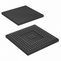
AT91SAM9XE256-CU Atmel, AT91SAM9XE256-CU Datasheet - Page 21

AT91SAM9XE256-CU
Manufacturer Part Number
AT91SAM9XE256-CU
Description
MCU ARM9 256K FLASH 217-BGA
Manufacturer
Atmel
Series
AT91SAMr
Specifications of AT91SAM9XE256-CU
Core Processor
ARM9
Core Size
16/32-Bit
Speed
180MHz
Connectivity
EBI/EMI, Ethernet, I²C, MMC, SPI, SSC, UART/USART, USB
Peripherals
Brown-out Detect/Reset, POR, PWM, WDT
Number Of I /o
96
Program Memory Size
256KB (256K x 8)
Program Memory Type
FLASH
Ram Size
56K x 8
Voltage - Supply (vcc/vdd)
1.65 V ~ 1.95 V
Data Converters
A/D 4x10b
Oscillator Type
Internal
Operating Temperature
-40°C ~ 85°C
Package / Case
217-LFBGA
Processor Series
AT91SAMx
Core
ARM926EJ-S
Data Bus Width
32 bit
Data Ram Size
32 KB
Interface Type
2-Wire, EBI, I2S, SPI, USART
Maximum Clock Frequency
180 MHz
Number Of Programmable I/os
96
Number Of Timers
6
Maximum Operating Temperature
+ 85 C
Mounting Style
SMD/SMT
3rd Party Development Tools
JTRACE-ARM-2M, KSK-AT91SAM9XE-PL, MDK-ARM, RL-ARM, ULINK2
Development Tools By Supplier
AT91SAM-ICE, AT91-ISP, AT91SAM9XE-EK
Minimum Operating Temperature
- 40 C
On-chip Adc
10 bit, 4 Channel
Package
217LFBGA
Device Core
ARM926EJ-S
Family Name
91S
Maximum Speed
180 MHz
Operating Supply Voltage
1.8|2.5|3.3 V
For Use With
AT91SAM9XE-EK - KIT EVAL FOR AT91SAM9XEAT91SAM-ICE - EMULATOR FOR AT91 ARM7/ARM9
Lead Free Status / RoHS Status
Lead free / RoHS Compliant
Eeprom Size
-
Lead Free Status / Rohs Status
Lead free / RoHS Compliant
Available stocks
Company
Part Number
Manufacturer
Quantity
Price
Company:
Part Number:
AT91SAM9XE256-CU
Manufacturer:
ATMEL
Quantity:
215
- Current page: 21 of 860
- Download datasheet (13Mb)
8.1
8.1.1
8.1.2
8.1.3
8.1.4
6254C–ATARM–22-Jan-10
Embedded Memories
AT91SAM9XE128
AT91SAM9XE256
AT91SAM9XE512
ROM Topology
A first level of address decoding is performed by the Bus Matrix, i.e., the implementation of the
Advanced High performance Bus (AHB) for its Master and Slave interfaces with additional
features.
Decoding breaks up the 4 Gbytes of address space into 16 banks of 256 Mbytes. The banks 1 to
7 are directed to the EBI that associates these banks to the external chip selects EBI_NCS0 to
EBI_NCS7. Bank 0 is reserved for the addressing of the internal memories, and a second level
of decoding provides 1 Mbyte of internal memory area. Bank 15 is reserved for the peripherals
and provides access to the Advanced Peripheral Bus (APB).
Other areas are unused and performing an access within them provides an abort to the master
requesting such an access.
Each Master has its own bus and its own decoder, thus allowing a different memory mapping
per Master. However, in order to simplify the mappings, all the masters have a similar address
decoding.
Regarding Master 0 and Master 1 (ARM926 Instruction and Data), three different Slaves are
assigned to the memory space decoded at address 0x0: one for internal boot, one for external
boot, one after remap, refer to
A complete memory map is presented in
The embedded ROM contains the Fast Flash Programming and the SAM-BA boot programs.
Each of these two programs is stored on 16-Kbyte Boundary of FFPI and the program executed
• 32 Kbytes ROM
• 16 Kbytes Fast SRAM
• 128 Kbytes Embedded Flash
• 32 Kbytes ROM
• 32 Kbytes Fast SRAM
• 256 Kbytes Embedded Flash
• 32 Kbytes ROM
• 32 Kbytes Fast SRAM
• 512 Kbytes Embedded Flash
– Single Cycle Access at full matrix speed
– Single Cycle Access at full matrix speed
– Single Cycle Access at full matrix speed
– Single Cycle Access at full matrix speed
– Single Cycle Access at full matrix speed
– Single Cycle Access at full matrix speed
AT91SAM9XE128/256/512 Preliminary
Table 8-3, “Internal Memory Mapping,” on page 25
Figure 8-1 on page
20.
for details.
21
Related parts for AT91SAM9XE256-CU
Image
Part Number
Description
Manufacturer
Datasheet
Request
R

Part Number:
Description:
KIT EVAL FOR AT91SAM9XE
Manufacturer:
Atmel
Datasheet:

Part Number:
Description:
MCU ARM9 64K SRAM 144-LFBGA
Manufacturer:
Atmel
Datasheet:

Part Number:
Description:
IC ARM7 MCU FLASH 256K 100LQFP
Manufacturer:
Atmel
Datasheet:

Part Number:
Description:
IC ARM9 MPU 217-LFBGA
Manufacturer:
Atmel
Datasheet:

Part Number:
Description:
MCU ARM9 ULTRA LOW PWR 217-LFBGA
Manufacturer:
Atmel
Datasheet:

Part Number:
Description:
MCU ARM9 324-TFBGA
Manufacturer:
Atmel
Datasheet:

Part Number:
Description:
IC MCU ARM9 SAMPLING 217CBGA
Manufacturer:
Atmel
Datasheet:

Part Number:
Description:
IC ARM9 MCU 217-LFBGA
Manufacturer:
Atmel
Datasheet:

Part Number:
Description:
IC ARM9 MCU 208-PQFP
Manufacturer:
Atmel
Datasheet:

Part Number:
Description:
MCU ARM 512K HS FLASH 100-LQFP
Manufacturer:
Atmel
Datasheet:

Part Number:
Description:
MCU ARM 512K HS FLASH 100-TFBGA
Manufacturer:
Atmel
Datasheet:

Part Number:
Description:
IC ARM9 MCU 200 MHZ 324-TFBGA
Manufacturer:
Atmel
Datasheet:

Part Number:
Description:
IC ARM MCU 16BIT 128K 256BGA
Manufacturer:
Atmel
Datasheet:

Part Number:
Description:
IC ARM7 MCU 32BIT 128K 64LQFP
Manufacturer:
Atmel
Datasheet:

Part Number:
Description:
IC ARM7 MCU FLASH 256K 128-LQFP
Manufacturer:
Atmel
Datasheet:


