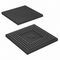
AT91SAM9XE256-CU Atmel, AT91SAM9XE256-CU Datasheet - Page 178

AT91SAM9XE256-CU
Manufacturer Part Number
AT91SAM9XE256-CU
Description
MCU ARM9 256K FLASH 217-BGA
Manufacturer
Atmel
Series
AT91SAMr
Specifications of AT91SAM9XE256-CU
Core Processor
ARM9
Core Size
16/32-Bit
Speed
180MHz
Connectivity
EBI/EMI, Ethernet, I²C, MMC, SPI, SSC, UART/USART, USB
Peripherals
Brown-out Detect/Reset, POR, PWM, WDT
Number Of I /o
96
Program Memory Size
256KB (256K x 8)
Program Memory Type
FLASH
Ram Size
56K x 8
Voltage - Supply (vcc/vdd)
1.65 V ~ 1.95 V
Data Converters
A/D 4x10b
Oscillator Type
Internal
Operating Temperature
-40°C ~ 85°C
Package / Case
217-LFBGA
Processor Series
AT91SAMx
Core
ARM926EJ-S
Data Bus Width
32 bit
Data Ram Size
32 KB
Interface Type
2-Wire, EBI, I2S, SPI, USART
Maximum Clock Frequency
180 MHz
Number Of Programmable I/os
96
Number Of Timers
6
Maximum Operating Temperature
+ 85 C
Mounting Style
SMD/SMT
3rd Party Development Tools
JTRACE-ARM-2M, KSK-AT91SAM9XE-PL, MDK-ARM, RL-ARM, ULINK2
Development Tools By Supplier
AT91SAM-ICE, AT91-ISP, AT91SAM9XE-EK
Minimum Operating Temperature
- 40 C
On-chip Adc
10 bit, 4 Channel
Package
217LFBGA
Device Core
ARM926EJ-S
Family Name
91S
Maximum Speed
180 MHz
Operating Supply Voltage
1.8|2.5|3.3 V
For Use With
AT91SAM9XE-EK - KIT EVAL FOR AT91SAM9XEAT91SAM-ICE - EMULATOR FOR AT91 ARM7/ARM9
Lead Free Status / RoHS Status
Lead free / RoHS Compliant
Eeprom Size
-
Lead Free Status / Rohs Status
Lead free / RoHS Compliant
Available stocks
Company
Part Number
Manufacturer
Quantity
Price
Company:
Part Number:
AT91SAM9XE256-CU
Manufacturer:
ATMEL
Quantity:
215
- Current page: 178 of 860
- Download datasheet (13Mb)
22.6.6.1
22.6.6.2
178
AT91SAM9XE128/256/512 Preliminary
I/O Mode, Common Memory Mode, Attribute Memory Mode and True IDE Mode
CFCE1 and CFCE2 Signals
Within the NCS4 and/or NCS5 address space, the current transfer address is used to distinguish
I/O mode, common memory mode, attribute memory mode and True IDE mode.
The different modes are accessed through a specific memory mapping as illustrated on
22-3. A[23:21] bits of the transfer address are used to select the desired mode as described in
Table 22-5 on page
Figure 22-3. CompactFlash Memory Mapping
Note:
Table 22-5.
To cover all types of access, the SMC must be alternatively set to drive 8-bit data bus or 16-bit
data bus. The odd byte access on the D[7:0] bus is only possible when the SMC is configured to
drive 8-bit memory devices on the corresponding NCS pin (NCS4 or NCS5). The Chip Select
Register (DBW field in the corresponding Chip Select Register) of the NCS4 and/or NCS5
address space must be set as shown in
NBS1 and NBS0 are the byte selection signals from SMC and are available when the SMC is set
in Byte Select mode on the corresponding Chip Select.
A[23:21]
000
010
100
110
111
The A22 pin is used to drive the REG signal of the CompactFlash Device (except in True IDE
mode).
CF Address Space
CompactFlash Mode Selection
178.
Offset 0x00E0 0000
Offset 0x00C0 0000
Offset 0x0080 0000
Offset 0x0040 0000
Offset 0x0000 0000
Table 22-6
to enable the required access type.
Alternate True IDE Mode
Mode Base Address
Common Memory Mode Space
Common Memory
True IDE Alternate Mode Space
Attribute Memory Mode Space
Attribute Memory
True IDE Mode
True IDE Mode Space
I/O Mode
I/O Mode Space
6254C–ATARM–22-Jan-10
Figure
Related parts for AT91SAM9XE256-CU
Image
Part Number
Description
Manufacturer
Datasheet
Request
R

Part Number:
Description:
KIT EVAL FOR AT91SAM9XE
Manufacturer:
Atmel
Datasheet:

Part Number:
Description:
MCU ARM9 64K SRAM 144-LFBGA
Manufacturer:
Atmel
Datasheet:

Part Number:
Description:
IC ARM7 MCU FLASH 256K 100LQFP
Manufacturer:
Atmel
Datasheet:

Part Number:
Description:
IC ARM9 MPU 217-LFBGA
Manufacturer:
Atmel
Datasheet:

Part Number:
Description:
MCU ARM9 ULTRA LOW PWR 217-LFBGA
Manufacturer:
Atmel
Datasheet:

Part Number:
Description:
MCU ARM9 324-TFBGA
Manufacturer:
Atmel
Datasheet:

Part Number:
Description:
IC MCU ARM9 SAMPLING 217CBGA
Manufacturer:
Atmel
Datasheet:

Part Number:
Description:
IC ARM9 MCU 217-LFBGA
Manufacturer:
Atmel
Datasheet:

Part Number:
Description:
IC ARM9 MCU 208-PQFP
Manufacturer:
Atmel
Datasheet:

Part Number:
Description:
MCU ARM 512K HS FLASH 100-LQFP
Manufacturer:
Atmel
Datasheet:

Part Number:
Description:
MCU ARM 512K HS FLASH 100-TFBGA
Manufacturer:
Atmel
Datasheet:

Part Number:
Description:
IC ARM9 MCU 200 MHZ 324-TFBGA
Manufacturer:
Atmel
Datasheet:

Part Number:
Description:
IC ARM MCU 16BIT 128K 256BGA
Manufacturer:
Atmel
Datasheet:

Part Number:
Description:
IC ARM7 MCU 32BIT 128K 64LQFP
Manufacturer:
Atmel
Datasheet:

Part Number:
Description:
IC ARM7 MCU FLASH 256K 128-LQFP
Manufacturer:
Atmel
Datasheet:


