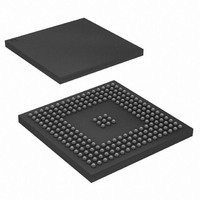
AT91SAM9XE256-CU Atmel, AT91SAM9XE256-CU Datasheet - Page 324

AT91SAM9XE256-CU
Manufacturer Part Number
AT91SAM9XE256-CU
Description
MCU ARM9 256K FLASH 217-BGA
Manufacturer
Atmel
Series
AT91SAMr
Specifications of AT91SAM9XE256-CU
Core Processor
ARM9
Core Size
16/32-Bit
Speed
180MHz
Connectivity
EBI/EMI, Ethernet, I²C, MMC, SPI, SSC, UART/USART, USB
Peripherals
Brown-out Detect/Reset, POR, PWM, WDT
Number Of I /o
96
Program Memory Size
256KB (256K x 8)
Program Memory Type
FLASH
Ram Size
56K x 8
Voltage - Supply (vcc/vdd)
1.65 V ~ 1.95 V
Data Converters
A/D 4x10b
Oscillator Type
Internal
Operating Temperature
-40°C ~ 85°C
Package / Case
217-LFBGA
Processor Series
AT91SAMx
Core
ARM926EJ-S
Data Bus Width
32 bit
Data Ram Size
32 KB
Interface Type
2-Wire, EBI, I2S, SPI, USART
Maximum Clock Frequency
180 MHz
Number Of Programmable I/os
96
Number Of Timers
6
Maximum Operating Temperature
+ 85 C
Mounting Style
SMD/SMT
3rd Party Development Tools
JTRACE-ARM-2M, KSK-AT91SAM9XE-PL, MDK-ARM, RL-ARM, ULINK2
Development Tools By Supplier
AT91SAM-ICE, AT91-ISP, AT91SAM9XE-EK
Minimum Operating Temperature
- 40 C
On-chip Adc
10 bit, 4 Channel
Package
217LFBGA
Device Core
ARM926EJ-S
Family Name
91S
Maximum Speed
180 MHz
Operating Supply Voltage
1.8|2.5|3.3 V
For Use With
AT91SAM9XE-EK - KIT EVAL FOR AT91SAM9XEAT91SAM-ICE - EMULATOR FOR AT91 ARM7/ARM9
Lead Free Status / RoHS Status
Lead free / RoHS Compliant
Eeprom Size
-
Lead Free Status / Rohs Status
Lead free / RoHS Compliant
Available stocks
Company
Part Number
Manufacturer
Quantity
Price
Company:
Part Number:
AT91SAM9XE256-CU
Manufacturer:
ATMEL
Quantity:
215
- Current page: 324 of 860
- Download datasheet (13Mb)
6254C–ATARM–22-Jan-10
4. Setting PLL B and divider B:
5. Selection of Master Clock and Processor Clock
waiting the interrupt line to be raised if the associated interrupt to LOCKA has been enabled
in the PMC_IER register.
All parameters in CKGR_PLLAR can be programmed in a single write operation. If at some
stage one of the following parameters, SRCA, MULA, DIVA is modified, LOCKA bit will go
low to indicate that PLL A is not ready yet. When PLL A is locked, LOCKA will be set again.
User has to wait for LOCKA bit to be set before using the PLL A output clock.
Code Example:
PLL A and divider A are enabled. PLL A input clock is main clock divided by 5. PLL An out-
put clock is PLL A input clock multiplied by 4. Once CKGR_PLLAR has been written,
LOCKA bit will be set after six slow clock cycles.
All parameters needed to configure PLL B and divider B are located in the CKGR_PLLBR
register. ICPPLLB in PMC_PLLICPR register must be set to 1 before configuring the
CKGR_PLLBR register.
The DIVB field is used to control divider B itself. A value between 0 and 255 can be pro-
grammed. Divider B output is divider B input divided by DIVB parameter. By default DIVB
parameter is set to 0 which means that divider B is turned off.
The OUTB field is used to select the PLL B output frequency range.
The MULB field is the PLL B multiplier factor. This parameter can be programmed between
0 and 2047. If MULB is set to 0, PLL B will be turned off, otherwise the PLL B output fre-
quency is PLL B input frequency multiplied by (MULB + 1).
The PLLBCOUNT field specifies the number of slow clock cycles before LOCKB bit is set in
the PMC_SR register after CKGR_PLLBR register has been written.
Once the PMC_PLLB register has been written, the user must wait for the LOCKB bit to be
set in the PMC_SR register. This can be done either by polling the status register or by wait-
ing the interrupt line to be raised if the associated interrupt to LOCKB has been enabled in
the PMC_IER register. All parameters in CKGR_PLLBR can be programmed in a single
write operation. If at some stage one of the following parameters, MULB, DIVB is modified,
LOCKB bit will go low to indicate that PLL B is not ready yet. When PLL B is locked, LOCKB
will be set again. The user is constrained to wait for LOCKB bit to be set before using the
PLL A output clock.
The USBDIV field is used to control the additional divider by 1, 2 or 4, which generates the
USB clock(s).
Code Example:
If PLL B and divider B are enabled, the PLL B input clock is the main clock. PLL B output
clock is PLL B input clock multiplied by 5. Once CKGR_PLLBR has been written, LOCKB bit
will be set after eight slow clock cycles.
The Master Clock and the Processor Clock are configurable via the PMC_MCKR register.
write_register(CKGR_PLLAR,0x20030605)
write_register(CKGR_PLLBR,0x00040805)
AT91SAM9XE128/256/512 Preliminary
324
Related parts for AT91SAM9XE256-CU
Image
Part Number
Description
Manufacturer
Datasheet
Request
R

Part Number:
Description:
KIT EVAL FOR AT91SAM9XE
Manufacturer:
Atmel
Datasheet:

Part Number:
Description:
MCU ARM9 64K SRAM 144-LFBGA
Manufacturer:
Atmel
Datasheet:

Part Number:
Description:
IC ARM7 MCU FLASH 256K 100LQFP
Manufacturer:
Atmel
Datasheet:

Part Number:
Description:
IC ARM9 MPU 217-LFBGA
Manufacturer:
Atmel
Datasheet:

Part Number:
Description:
MCU ARM9 ULTRA LOW PWR 217-LFBGA
Manufacturer:
Atmel
Datasheet:

Part Number:
Description:
MCU ARM9 324-TFBGA
Manufacturer:
Atmel
Datasheet:

Part Number:
Description:
IC MCU ARM9 SAMPLING 217CBGA
Manufacturer:
Atmel
Datasheet:

Part Number:
Description:
IC ARM9 MCU 217-LFBGA
Manufacturer:
Atmel
Datasheet:

Part Number:
Description:
IC ARM9 MCU 208-PQFP
Manufacturer:
Atmel
Datasheet:

Part Number:
Description:
MCU ARM 512K HS FLASH 100-LQFP
Manufacturer:
Atmel
Datasheet:

Part Number:
Description:
MCU ARM 512K HS FLASH 100-TFBGA
Manufacturer:
Atmel
Datasheet:

Part Number:
Description:
IC ARM9 MCU 200 MHZ 324-TFBGA
Manufacturer:
Atmel
Datasheet:

Part Number:
Description:
IC ARM MCU 16BIT 128K 256BGA
Manufacturer:
Atmel
Datasheet:

Part Number:
Description:
IC ARM7 MCU 32BIT 128K 64LQFP
Manufacturer:
Atmel
Datasheet:

Part Number:
Description:
IC ARM7 MCU FLASH 256K 128-LQFP
Manufacturer:
Atmel
Datasheet:


