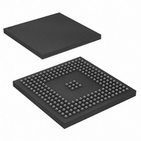
AT91SAM9XE256-CU Atmel, AT91SAM9XE256-CU Datasheet - Page 244

AT91SAM9XE256-CU
Manufacturer Part Number
AT91SAM9XE256-CU
Description
MCU ARM9 256K FLASH 217-BGA
Manufacturer
Atmel
Series
AT91SAMr
Specifications of AT91SAM9XE256-CU
Core Processor
ARM9
Core Size
16/32-Bit
Speed
180MHz
Connectivity
EBI/EMI, Ethernet, I²C, MMC, SPI, SSC, UART/USART, USB
Peripherals
Brown-out Detect/Reset, POR, PWM, WDT
Number Of I /o
96
Program Memory Size
256KB (256K x 8)
Program Memory Type
FLASH
Ram Size
56K x 8
Voltage - Supply (vcc/vdd)
1.65 V ~ 1.95 V
Data Converters
A/D 4x10b
Oscillator Type
Internal
Operating Temperature
-40°C ~ 85°C
Package / Case
217-LFBGA
Processor Series
AT91SAMx
Core
ARM926EJ-S
Data Bus Width
32 bit
Data Ram Size
32 KB
Interface Type
2-Wire, EBI, I2S, SPI, USART
Maximum Clock Frequency
180 MHz
Number Of Programmable I/os
96
Number Of Timers
6
Maximum Operating Temperature
+ 85 C
Mounting Style
SMD/SMT
3rd Party Development Tools
JTRACE-ARM-2M, KSK-AT91SAM9XE-PL, MDK-ARM, RL-ARM, ULINK2
Development Tools By Supplier
AT91SAM-ICE, AT91-ISP, AT91SAM9XE-EK
Minimum Operating Temperature
- 40 C
On-chip Adc
10 bit, 4 Channel
Package
217LFBGA
Device Core
ARM926EJ-S
Family Name
91S
Maximum Speed
180 MHz
Operating Supply Voltage
1.8|2.5|3.3 V
For Use With
AT91SAM9XE-EK - KIT EVAL FOR AT91SAM9XEAT91SAM-ICE - EMULATOR FOR AT91 ARM7/ARM9
Lead Free Status / RoHS Status
Lead free / RoHS Compliant
Eeprom Size
-
Lead Free Status / Rohs Status
Lead free / RoHS Compliant
Available stocks
Company
Part Number
Manufacturer
Quantity
Price
Company:
Part Number:
AT91SAM9XE256-CU
Manufacturer:
ATMEL
Quantity:
215
- Current page: 244 of 860
- Download datasheet (13Mb)
24.5
24.5.1
Figure 24-2. Write Burst, 32-bit SDRAM Access
SDRAMC_A[12:0]
24.5.2
6254C–ATARM–22-Jan-10
D[31:0]
SDWE
SDCS
SDCK
Functional Description
RAS
CAS
SDRAM Controller Write Cycle
SDRAM Controller Read Cycle
Row n
The SDRAM Controller allows burst access or single access. In both cases, the SDRAM control-
ler keeps track of the active row in each bank, thus maximizing performance. To initiate a burst
access, the SDRAM Controller uses the transfer type signal provided by the master requesting
the access. If the next access is a sequential write access, writing to the SDRAM device is car-
ried out. If the next access is a write-sequential access, but the current access is to a boundary
page, or if the next access is in another row, then the SDRAM Controller generates a precharge
command, activates the new row and initiates a write command. To comply with SDRAM timing
parameters, additional clock cycles are inserted between precharge/active (t
active/write (t
Configuration Register” on page
The SDRAM Controller allows burst access, incremental burst of unspecified length or single
access. In all cases, the SDRAM Controller keeps track of the active row in each bank, thus
maximizing performance of the SDRAM. If row and bank addresses do not match the previous
row/bank address, then the SDRAM controller automatically generates a precharge command,
activates the new row and starts the read command. To comply with the SDRAM timing param-
eters, additional clock cycles on SDCK are inserted between precharge and active commands
(t
uration register of the SDRAM Controller. After a read command, additional wait states are
generated to comply with the CAS latency (1, 2 or 3 clock delays specified in the configuration
register).
RP
) and between active and read command (t
t
RCD
= 3
col a
RCD
Dna
) commands. For definition of these timing parameters, refer to the
col b
Dnb
AT91SAM9XE128/256/512 Preliminary
col c
Dnc
254. This is described in
col d
Dnd
col e
Dne
RCD
col f
Dnf
). These two parameters are set in the config-
col g
Dng
Figure 24-2
col h
Dnh
col i
Dni
below.
col j
Dnj
RP
) commands and
col k
Dnk
“SDRAMC
col l
Dnl
244
Related parts for AT91SAM9XE256-CU
Image
Part Number
Description
Manufacturer
Datasheet
Request
R

Part Number:
Description:
KIT EVAL FOR AT91SAM9XE
Manufacturer:
Atmel
Datasheet:

Part Number:
Description:
MCU ARM9 64K SRAM 144-LFBGA
Manufacturer:
Atmel
Datasheet:

Part Number:
Description:
IC ARM7 MCU FLASH 256K 100LQFP
Manufacturer:
Atmel
Datasheet:

Part Number:
Description:
IC ARM9 MPU 217-LFBGA
Manufacturer:
Atmel
Datasheet:

Part Number:
Description:
MCU ARM9 ULTRA LOW PWR 217-LFBGA
Manufacturer:
Atmel
Datasheet:

Part Number:
Description:
MCU ARM9 324-TFBGA
Manufacturer:
Atmel
Datasheet:

Part Number:
Description:
IC MCU ARM9 SAMPLING 217CBGA
Manufacturer:
Atmel
Datasheet:

Part Number:
Description:
IC ARM9 MCU 217-LFBGA
Manufacturer:
Atmel
Datasheet:

Part Number:
Description:
IC ARM9 MCU 208-PQFP
Manufacturer:
Atmel
Datasheet:

Part Number:
Description:
MCU ARM 512K HS FLASH 100-LQFP
Manufacturer:
Atmel
Datasheet:

Part Number:
Description:
MCU ARM 512K HS FLASH 100-TFBGA
Manufacturer:
Atmel
Datasheet:

Part Number:
Description:
IC ARM9 MCU 200 MHZ 324-TFBGA
Manufacturer:
Atmel
Datasheet:

Part Number:
Description:
IC ARM MCU 16BIT 128K 256BGA
Manufacturer:
Atmel
Datasheet:

Part Number:
Description:
IC ARM7 MCU 32BIT 128K 64LQFP
Manufacturer:
Atmel
Datasheet:

Part Number:
Description:
IC ARM7 MCU FLASH 256K 128-LQFP
Manufacturer:
Atmel
Datasheet:


