AT32UC3B1256-AUR Atmel, AT32UC3B1256-AUR Datasheet - Page 606
AT32UC3B1256-AUR
Manufacturer Part Number
AT32UC3B1256-AUR
Description
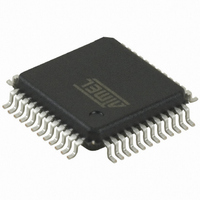
MCU AVR32 256K FLASH 48-TQFP
Manufacturer
Atmel
Series
AVR®32 UC3r
Datasheet
1.AT32UC3B164-AUR.pdf
(680 pages)
Specifications of AT32UC3B1256-AUR
Package / Case
48-TQFP, 48-VQFP
Voltage - Supply (vcc/vdd)
1.65 V ~ 1.95 V
Operating Temperature
-40°C ~ 85°C
Speed
60MHz
Number Of I /o
28
Core Processor
AVR
Program Memory Type
FLASH
Ram Size
32K x 8
Program Memory Size
256KB (256K x 8)
Data Converters
A/D 6x10b
Oscillator Type
Internal
Peripherals
Brown-out Detect/Reset, DMA, POR, PWM, WDT
Connectivity
I²C, IrDA, SPI, SSC, UART/USART, USB
Core Size
32-Bit
Lead Free Status / RoHS Status
Lead free / RoHS Compliant
Eeprom Size
-
Available stocks
Company
Part Number
Manufacturer
Quantity
Price
Company:

Part Number:
AT32UC3B1256-AUR
Manufacturer:
OMRON
Quantity:
12 000


27.5.2.4
27.5.2.5
32059J–12/2010
INTEST
CLAMP
This instruction selects the boundary-scan chain as Data Register for testing internal logic in the
device. The logic inputs are determined by the boundary-scan chain, and the logic outputs are
captured by the boundary-scan chain. The device output pins are driven from the boundary-scan
chain.
Starting in Run-Test/Idle, the INTEST instruction is accessed the following way:
1. Select the IR Scan path.
2. In Capture-IR: The IR output value is latched into the shift register.
3. In Shift-IR: The instruction register is shifted by the TCK input.
4. In Update-IR: The data from the boundary-scan chain is applied to the internal logic
5. Return to Run-Test/Idle.
6. Select the DR Scan path.
7. In Capture-DR: The data on the internal logic is sampled into the boundary-scan chain.
8. In Shift-DR: The boundary-scan chain is shifted by the TCK input.
9. In Update-DR: The data from the boundary-scan chain is applied to internal logic inputs.
10. Return to Run-Test/Idle.
Table 27-13. INTEST Details
This instruction selects the Bypass register as Data Register. The device output pins are driven
from the boundary-scan chain.
Starting in Run-Test/Idle, the CLAMP instruction is accessed the following way:
1. Select the IR Scan path.
2. In Capture-IR: The IR output value is latched into the shift register.
3. In Shift-IR: The instruction register is shifted by the TCK input.
4. In Update-IR: The data from the boundary-scan chain is applied to the output pins.
5. Return to Run-Test/Idle.
6. Select the DR Scan path.
7. In Capture-DR: A logic ‘0’ is loaded into the Bypass Register.
8. In Shift-DR: Data is scanned from TDI to TDO through the Bypass register.
Instructions
IR input value
IR output value
DR Size
DR input value
DR output value
inputs.
Details
00100 (0x04)
p0001
Depending on boundary-scan chain, see BSDL-file.
Depending on boundary-scan chain, see BSDL-file.
Depending on boundary-scan chain, see BSDL-file.
AT32UC3B
606
Related parts for AT32UC3B1256-AUR
Image
Part Number
Description
Manufacturer
Datasheet
Request
R

Part Number:
Description:
DEV KIT FOR AVR/AVR32
Manufacturer:
Atmel
Datasheet:

Part Number:
Description:
INTERVAL AND WIPE/WASH WIPER CONTROL IC WITH DELAY
Manufacturer:
ATMEL Corporation
Datasheet:
Part Number:
Description:
Low-Voltage Voice-Switched IC for Hands-Free Operation
Manufacturer:
ATMEL Corporation
Datasheet:
Part Number:
Description:
MONOLITHIC INTEGRATED FEATUREPHONE CIRCUIT
Manufacturer:
ATMEL Corporation
Datasheet:
Part Number:
Description:
AM-FM Receiver IC U4255BM-M
Manufacturer:
ATMEL Corporation
Datasheet:
Part Number:
Description:
Monolithic Integrated Feature Phone Circuit
Manufacturer:
ATMEL Corporation
Datasheet:
Part Number:
Description:
Multistandard Video-IF and Quasi Parallel Sound Processing
Manufacturer:
ATMEL Corporation
Datasheet:
Part Number:
Description:
High-performance EE PLD
Manufacturer:
ATMEL Corporation
Datasheet:
Part Number:
Description:
8-bit Flash Microcontroller
Manufacturer:
ATMEL Corporation
Datasheet:
Part Number:
Description:
2-Wire Serial EEPROM
Manufacturer:
ATMEL Corporation
Datasheet: