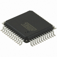
AT32UC3B1256-AUR Atmel, AT32UC3B1256-AUR Datasheet - Page 39

AT32UC3B1256-AUR
Manufacturer Part Number
AT32UC3B1256-AUR
Description
MCU AVR32 256K FLASH 48-TQFP
Manufacturer
Atmel
Series
AVR®32 UC3r
Datasheet
1.AT32UC3B164-AUR.pdf
(680 pages)
Specifications of AT32UC3B1256-AUR
Package / Case
48-TQFP, 48-VQFP
Voltage - Supply (vcc/vdd)
1.65 V ~ 1.95 V
Operating Temperature
-40°C ~ 85°C
Speed
60MHz
Number Of I /o
28
Core Processor
AVR
Program Memory Type
FLASH
Ram Size
32K x 8
Program Memory Size
256KB (256K x 8)
Data Converters
A/D 6x10b
Oscillator Type
Internal
Peripherals
Brown-out Detect/Reset, DMA, POR, PWM, WDT
Connectivity
I²C, IrDA, SPI, SSC, UART/USART, USB
Core Size
32-Bit
Lead Free Status / RoHS Status
Lead free / RoHS Compliant
Eeprom Size
-
Available stocks
Company
Part Number
Manufacturer
Quantity
Price
Company:
Part Number:
AT32UC3B1256-AUR
Manufacturer:
OMRON
Quantity:
12 000
- Current page: 39 of 680
- Download datasheet (10Mb)
O s c 1
c lo c k
O s c 0
9.5.4.1
9.5.5
32059J–12/2010
c lo c k
P L L O S C
0
1
Synchronous clocks
Enabling the PLL
D iv id e r
P L L D I V
I n p u t
When the PLL is switched on, or when changing the clock source or multiplication factor for the
PLL, the PLL is unlocked and the output frequency is undefined. The PLL clock for the digital
logic is automatically masked when the PLL is unlocked, to prevent connected digital logic from
receiving a too high frequency and thus become unstable.
Figure 9-3.
PLLn is enabled by writing the PLLEN bit in the PLLn register. PLLOSC selects Oscillator 0 or 1
as clock source. The PLLMUL and PLLDIV bitfields must be written with the multiplication and
division factors, respectively, creating the voltage controlled ocillator frequency f
frequency f
If PLLOPT[1] field is set to 0:
If PLLOPT[1] field is set to 1:
The PLLn:PLLOPT field should be set to proper values according to the PLL operating fre-
quency. The PLLOPT field can also be set to divide the output frequency of the PLLs by 2.
The lock signal for each PLL is available as a LOCKn flag in POSCSR. An interrupt can be gen-
erated on a 0 to 1 transition of these bits.
The slow clock (default), Oscillator 0, or PLL0 provide the source for the main clock, which is the
common root for the synchronous clocks for the CPU/HSB, PBA, and PBB modules. The main
clock is divided by an 8-bit prescaler, and each of these four synchronous clocks can run from
f
f
f
f
VCO
VCO
PLL
PLL
= f
= f
= (PLLMUL+1)/(PLLDIV) • f
= 2*(PLLMUL+1) • f
PLL
D iv id e r
O u t p u t
D e t e c t o r
P L L M U L
VCO.
VCO
P h a s e
PLL with control logic and filters
:
/ 2
.
P L L O P T
V C O
OSC
if PLLDIV = 0.
f
OSC
v c o
if PLLDIV > 0.
D e t e c t o r
1 / 2
L o c k
P L L O P T [ 1 ]
0
1
f
P L L
M a s k
AT32UC3B
VCO
L o c k b it
and the PLL
P L L c lo c k
39
Related parts for AT32UC3B1256-AUR
Image
Part Number
Description
Manufacturer
Datasheet
Request
R

Part Number:
Description:
DEV KIT FOR AVR/AVR32
Manufacturer:
Atmel
Datasheet:

Part Number:
Description:
INTERVAL AND WIPE/WASH WIPER CONTROL IC WITH DELAY
Manufacturer:
ATMEL Corporation
Datasheet:

Part Number:
Description:
Low-Voltage Voice-Switched IC for Hands-Free Operation
Manufacturer:
ATMEL Corporation
Datasheet:

Part Number:
Description:
MONOLITHIC INTEGRATED FEATUREPHONE CIRCUIT
Manufacturer:
ATMEL Corporation
Datasheet:

Part Number:
Description:
AM-FM Receiver IC U4255BM-M
Manufacturer:
ATMEL Corporation
Datasheet:

Part Number:
Description:
Monolithic Integrated Feature Phone Circuit
Manufacturer:
ATMEL Corporation
Datasheet:

Part Number:
Description:
Multistandard Video-IF and Quasi Parallel Sound Processing
Manufacturer:
ATMEL Corporation
Datasheet:

Part Number:
Description:
High-performance EE PLD
Manufacturer:
ATMEL Corporation
Datasheet:

Part Number:
Description:
8-bit Flash Microcontroller
Manufacturer:
ATMEL Corporation
Datasheet:

Part Number:
Description:
2-Wire Serial EEPROM
Manufacturer:
ATMEL Corporation
Datasheet:


