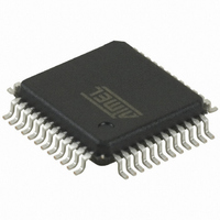
AT32UC3B1256-AUR Atmel, AT32UC3B1256-AUR Datasheet - Page 123

AT32UC3B1256-AUR
Manufacturer Part Number
AT32UC3B1256-AUR
Description
MCU AVR32 256K FLASH 48-TQFP
Manufacturer
Atmel
Series
AVR®32 UC3r
Datasheet
1.AT32UC3B164-AUR.pdf
(680 pages)
Specifications of AT32UC3B1256-AUR
Package / Case
48-TQFP, 48-VQFP
Voltage - Supply (vcc/vdd)
1.65 V ~ 1.95 V
Operating Temperature
-40°C ~ 85°C
Speed
60MHz
Number Of I /o
28
Core Processor
AVR
Program Memory Type
FLASH
Ram Size
32K x 8
Program Memory Size
256KB (256K x 8)
Data Converters
A/D 6x10b
Oscillator Type
Internal
Peripherals
Brown-out Detect/Reset, DMA, POR, PWM, WDT
Connectivity
I²C, IrDA, SPI, SSC, UART/USART, USB
Core Size
32-Bit
Lead Free Status / RoHS Status
Lead free / RoHS Compliant
Eeprom Size
-
Available stocks
Company
Part Number
Manufacturer
Quantity
Price
Company:
Part Number:
AT32UC3B1256-AUR
Manufacturer:
OMRON
Quantity:
12 000
- Current page: 123 of 680
- Download datasheet (10Mb)
14.4.5
14.4.6
32059J–12/2010
Quick Page Read
Write page buffer operations
The flash controller supports flash blocks with up to 2^21 word addresses, as displayed in
14-1. Reading the memory space between address pw and 2^21-1 returns an undefined result.
The User page is permanently mapped to word address 2^21.
Table 14-1.
Figure 14-1. Memory map for the Flash memories
A dedicated command, Quick Page Read (QPR), is provided to read all words in an addressed
page. All bits in all words in this page are AND’ed together, returning a 1-bit result. This result is
placed in the Quick Page Read Result (QPRR) bit in Flash Status Register (FSR). The QPR
command is useful to check that a page is in an erased state. The QPR instruction is much
faster than performing the erased-page check using a regular software subroutine.
The internal memory area reserved for the embedded flash can also be written through a write-
only page buffer. The page buffer is addressed only by the address bits required to address w
words (since the page buffer is word addressable) and thus wrap around within the internal
memory area address space and appear to be repeated within it.
When writing to the page buffer, the PAGEN field in the
updated with the page number corresponding to page address of the latest word written into the
page buffer.
Memory type
Main array
User
User page addresses
2 ^ 2 1 + 1 2 8
A ll a d d r e s s e s a r e w o r d a d d r e s s e s
Start address, byte sized
0
2^23 = 8388608
p w - 1
2 ^ 2 1
p w
F la s h w it h
e x t r a p a g e
0
U n u s e d
U s e r p a g e
Size
pw words = 4pw bytes
128 words = 512 bytes
Flash Command register (
AT32UC3B
FCMD) is
Figure
123
Related parts for AT32UC3B1256-AUR
Image
Part Number
Description
Manufacturer
Datasheet
Request
R

Part Number:
Description:
DEV KIT FOR AVR/AVR32
Manufacturer:
Atmel
Datasheet:

Part Number:
Description:
INTERVAL AND WIPE/WASH WIPER CONTROL IC WITH DELAY
Manufacturer:
ATMEL Corporation
Datasheet:

Part Number:
Description:
Low-Voltage Voice-Switched IC for Hands-Free Operation
Manufacturer:
ATMEL Corporation
Datasheet:

Part Number:
Description:
MONOLITHIC INTEGRATED FEATUREPHONE CIRCUIT
Manufacturer:
ATMEL Corporation
Datasheet:

Part Number:
Description:
AM-FM Receiver IC U4255BM-M
Manufacturer:
ATMEL Corporation
Datasheet:

Part Number:
Description:
Monolithic Integrated Feature Phone Circuit
Manufacturer:
ATMEL Corporation
Datasheet:

Part Number:
Description:
Multistandard Video-IF and Quasi Parallel Sound Processing
Manufacturer:
ATMEL Corporation
Datasheet:

Part Number:
Description:
High-performance EE PLD
Manufacturer:
ATMEL Corporation
Datasheet:

Part Number:
Description:
8-bit Flash Microcontroller
Manufacturer:
ATMEL Corporation
Datasheet:

Part Number:
Description:
2-Wire Serial EEPROM
Manufacturer:
ATMEL Corporation
Datasheet:


