AT32UC3B1256-AUR Atmel, AT32UC3B1256-AUR Datasheet - Page 179
AT32UC3B1256-AUR
Manufacturer Part Number
AT32UC3B1256-AUR
Description
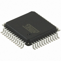
MCU AVR32 256K FLASH 48-TQFP
Manufacturer
Atmel
Series
AVR®32 UC3r
Datasheet
1.AT32UC3B164-AUR.pdf
(680 pages)
Specifications of AT32UC3B1256-AUR
Package / Case
48-TQFP, 48-VQFP
Voltage - Supply (vcc/vdd)
1.65 V ~ 1.95 V
Operating Temperature
-40°C ~ 85°C
Speed
60MHz
Number Of I /o
28
Core Processor
AVR
Program Memory Type
FLASH
Ram Size
32K x 8
Program Memory Size
256KB (256K x 8)
Data Converters
A/D 6x10b
Oscillator Type
Internal
Peripherals
Brown-out Detect/Reset, DMA, POR, PWM, WDT
Connectivity
I²C, IrDA, SPI, SSC, UART/USART, USB
Core Size
32-Bit
Lead Free Status / RoHS Status
Lead free / RoHS Compliant
Eeprom Size
-
Available stocks
Company
Part Number
Manufacturer
Quantity
Price
Company:

Part Number:
AT32UC3B1256-AUR
Manufacturer:
OMRON
Quantity:
12 000


17.6.1
32059J–12/2010
Access Types
Table 17-1.
1)
uration section at the end of this chapter.
2)
Each configuration register can be accessed in four different ways. The first address location
can be used to write the register directly. This address can also be used to read the register
value. The following addresses facilitate three different types of write access to the register. Per-
forming a “set” access, all bits written to one will be set. Bits written to zero will be unchanged by
the operation. Performing a “clear” access, all bits written to one will be cleared. Bits written to
zero will be unchanged by the operation. Finally, a toggle access will toggle the value of all bits
written to one. Again all bits written to zero remain unchanged. Note that for some registers (e.g.
IFR), not all access methods are permitted.
Note that for ports with less than 32 bits, the corresponding control registers will have unused
bits. This is also the case for features that are not implemented for a specific pin. Writing to an
unused bit will have no effect. Reading unused bits will always return 0.
Offset
0xBC
0xCC
0xDC
0xB4
0xB8
0xC0
0xC4
0xC8
0xD0
0xD4
0xD8
The reset value for these registers are device specific. Please refer to the Module Config-
The reset value is undefined depending on the pin states.
Glitch Filter Enable Register
Glitch Filter Enable Register
Glitch Filter Enable Register
Glitch Filter Enable Register
Interrupt Mode Register 1
Interrupt Mode Register 1
Interrupt Mode Register 1
Interrupt Flag Register
Interrupt Flag Register
Interrupt Flag Register
Interrupt Flag Register
GPIO Register Memory Map
Register
Read/Write
Function
Toggle
Toggle
Clear
Clear
Read
Clear
Set
Set
-
-
GFERS
GFERC
GFERT
IMR1S
IMR1C
IMR1T
GFER
Name
IFRC
IFR
-
-
Read/Write
Write-Only
Write-Only
Write-Only
Write-Only
Write-Only
Write-Only
Read-Only
Write-Only
Access
-
-
AT32UC3B
Reset value
(1)
(1)
179
Related parts for AT32UC3B1256-AUR
Image
Part Number
Description
Manufacturer
Datasheet
Request
R

Part Number:
Description:
DEV KIT FOR AVR/AVR32
Manufacturer:
Atmel
Datasheet:

Part Number:
Description:
INTERVAL AND WIPE/WASH WIPER CONTROL IC WITH DELAY
Manufacturer:
ATMEL Corporation
Datasheet:
Part Number:
Description:
Low-Voltage Voice-Switched IC for Hands-Free Operation
Manufacturer:
ATMEL Corporation
Datasheet:
Part Number:
Description:
MONOLITHIC INTEGRATED FEATUREPHONE CIRCUIT
Manufacturer:
ATMEL Corporation
Datasheet:
Part Number:
Description:
AM-FM Receiver IC U4255BM-M
Manufacturer:
ATMEL Corporation
Datasheet:
Part Number:
Description:
Monolithic Integrated Feature Phone Circuit
Manufacturer:
ATMEL Corporation
Datasheet:
Part Number:
Description:
Multistandard Video-IF and Quasi Parallel Sound Processing
Manufacturer:
ATMEL Corporation
Datasheet:
Part Number:
Description:
High-performance EE PLD
Manufacturer:
ATMEL Corporation
Datasheet:
Part Number:
Description:
8-bit Flash Microcontroller
Manufacturer:
ATMEL Corporation
Datasheet:
Part Number:
Description:
2-Wire Serial EEPROM
Manufacturer:
ATMEL Corporation
Datasheet: