DEMO9S08EL32 Freescale Semiconductor, DEMO9S08EL32 Datasheet - Page 79
DEMO9S08EL32
Manufacturer Part Number
DEMO9S08EL32
Description
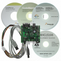
BOARD DEMO FOR 9S08 EL MCU
Manufacturer
Freescale Semiconductor
Type
MCUr
Datasheets
1.DEMO9S08EL32.pdf
(356 pages)
2.DEMO9S08EL32.pdf
(14 pages)
3.DEMO9S08EL32.pdf
(2 pages)
Specifications of DEMO9S08EL32
Contents
Evaluation Board
Processor To Be Evaluated
MC9S08EL32
Data Bus Width
8 bit
Interface Type
RS-232, USB
Operating Supply Voltage
12 V
Silicon Manufacturer
Freescale
Core Architecture
HCS08
Core Sub-architecture
HCS08
Silicon Core Number
MC9S08
Silicon Family Name
S08EL
Rohs Compliant
Yes
For Use With/related Products
MC9S08EL32
Lead Free Status / RoHS Status
Lead free / RoHS Compliant


Chapter 6
Parallel Input/Output Control
This section explains software controls related to parallel input/output (I/O) and pin control. The
MC9S08EL32 has three parallel I/O ports which include a total of 22 I/O pins. See
Connections,” for more information about pin assignments and external hardware considerations of these
pins.
Many of these pins are shared with on-chip peripherals such as timer systems, communication systems, or
keyboard interrupts as shown in
I/O functions so that when a peripheral is enabled, the I/O functions associated with the shared pins are
disabled.
After reset, the shared peripheral functions are disabled and the pins are configured as inputs
(PTxDDn = 0). The pin control functions for each pin are configured as follows: slew rate control enabled
(PTxSEn = 1), low drive strength selected (PTxDSn = 0), and internal pull-ups disabled (PTxPEn = 0).
6.1
Reading and writing of parallel I/Os are performed through the port data registers. The direction, either
input or output, is controlled through the port data direction registers. The parallel I/O port function for an
individual pin is illustrated in the block diagram shown in
The data direction control bit (PTxDDn) determines whether the output buffer for the associated pin is
enabled, and also controls the source for port data register reads. The input buffer for the associated pin is
always enabled unless the pin is enabled as an analog function or is an output-only pin.
When a shared digital function is enabled for a pin, the output buffer is controlled by the shared function.
However, the data direction register bit will continue to control the source for reads of the port data register.
When a shared analog function is enabled for a pin, both the input and output buffers are disabled. A value
of 0 is read for any port data bit where the bit is an input (PTxDDn = 0) and the input buffer is disabled. In
general, whenever a pin is shared with both an alternate digital function and an analog function, the analog
function has priority such that if both the digital and analog functions are enabled, the analog function
controls the pin.
Freescale Semiconductor
Port Data and Data Direction
Not all general-purpose I/O pins are available on all packages. To avoid
extra current drain from floating input pins, the user’s reset initialization
routine in the application program must either enable on-chip pull-up
devices or change the direction of unconnected pins to outputs so the pins
do not float.
MC9S08EL32 Series and MC9S08SL16 Series Data Sheet, Rev. 3
Table
2-1. The peripheral modules have priority over the general-purpose
NOTE
Figure
6-1.
Chapter 2, “Pins and
79
Related parts for DEMO9S08EL32
Image
Part Number
Description
Manufacturer
Datasheet
Request
R

Part Number:
Description:
Manufacturer:
Freescale Semiconductor, Inc
Datasheet:
Part Number:
Description:
Manufacturer:
Freescale Semiconductor, Inc
Datasheet:
Part Number:
Description:
Manufacturer:
Freescale Semiconductor, Inc
Datasheet:
Part Number:
Description:
Manufacturer:
Freescale Semiconductor, Inc
Datasheet:
Part Number:
Description:
Manufacturer:
Freescale Semiconductor, Inc
Datasheet:
Part Number:
Description:
Manufacturer:
Freescale Semiconductor, Inc
Datasheet:
Part Number:
Description:
Manufacturer:
Freescale Semiconductor, Inc
Datasheet:
Part Number:
Description:
Manufacturer:
Freescale Semiconductor, Inc
Datasheet:
Part Number:
Description:
Manufacturer:
Freescale Semiconductor, Inc
Datasheet:
Part Number:
Description:
Manufacturer:
Freescale Semiconductor, Inc
Datasheet:
Part Number:
Description:
Manufacturer:
Freescale Semiconductor, Inc
Datasheet:
Part Number:
Description:
Manufacturer:
Freescale Semiconductor, Inc
Datasheet:
Part Number:
Description:
Manufacturer:
Freescale Semiconductor, Inc
Datasheet:
Part Number:
Description:
Manufacturer:
Freescale Semiconductor, Inc
Datasheet:
Part Number:
Description:
Manufacturer:
Freescale Semiconductor, Inc
Datasheet: