DEMO9S08EL32 Freescale Semiconductor, DEMO9S08EL32 Datasheet - Page 55
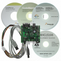
DEMO9S08EL32
Manufacturer Part Number
DEMO9S08EL32
Description
BOARD DEMO FOR 9S08 EL MCU
Manufacturer
Freescale Semiconductor
Type
MCUr
Datasheets
1.DEMO9S08EL32.pdf
(356 pages)
2.DEMO9S08EL32.pdf
(14 pages)
3.DEMO9S08EL32.pdf
(2 pages)
Specifications of DEMO9S08EL32
Contents
Evaluation Board
Processor To Be Evaluated
MC9S08EL32
Data Bus Width
8 bit
Interface Type
RS-232, USB
Operating Supply Voltage
12 V
Silicon Manufacturer
Freescale
Core Architecture
HCS08
Core Sub-architecture
HCS08
Silicon Core Number
MC9S08
Silicon Family Name
S08EL
Rohs Compliant
Yes
For Use With/related Products
MC9S08EL32
Lead Free Status / RoHS Status
Lead free / RoHS Compliant


4.5.10
Only half of the EEPROM is in the memory map. The EPGSEL bit in FCNFG register selects which half
of the array can be accessed in foreground while the other half can not be accessed in background. There
are two mapping mode options that can be selected to configure the 8-byte EEPROM sectors: 4-byte mode
and 8-byte mode. Each mode is selected by the EPGMOD bit in the FOPT register.
In 4-byte sector mode (EPGMOD = 0), each 8-byte sector splits four bytes on foreground and four bytes
on background but on the same addresses. The EPGSEL bit selects which four bytes can be accessed.
During a sector erase, the entire 8-byte sector (four bytes in foreground and four bytes in background) is
erased.
In 8-byte sector mode (EPGMOD = 1), each entire 8-byte sector is in a single page. The EPGSEL bit
selects which sectors are on background. During a sector erase, the entire 8-byte sector in foreground is
erased.
4.5.11
The FLASH and EEPROM module has seven 8-bit registers in the high-page register space and three
locations in the nonvolatile register space in FLASH memory. Two of those locations are copied into two
corresponding high-page control registers at reset. There is also an 8-byte comparison key in FLASH
memory. Refer to
EEPROM registers. This section refers to registers and control bits only by their names. A Freescale
Semiconductor-provided equate or header file normally is used to translate these names into the
appropriate absolute addresses.
4.5.11.1
Before any erase or programming operations are possible, write to this register to set the frequency of the
clock for the nonvolatile memory system within acceptable limits. Bit 7 is a read-only flag and bits 0 to 6
may be read at any time but can be written only one time after reset.
Freescale Semiconductor
Reset
W
R
DIVLD
EEPROM Mapping
FLASH and EEPROM Registers and Control Bits
FLASH and EEPROM Clock Divider Register (FCDIV)
0
7
Table 4-3
= Unimplemented or Reserved
Figure 4-5. FLASH and EEPROM Clock Divider Register (FCDIV)
PRDIV8
MC9S08EL32 Series and MC9S08SL16 Series Data Sheet, Rev. 3
0
6
and
Table 4-4
0
5
for the absolute address assignments for all FLASH and
0
4
3
0
DIV
0
2
0
1
Chapter 4 Memory
0
0
55
Related parts for DEMO9S08EL32
Image
Part Number
Description
Manufacturer
Datasheet
Request
R

Part Number:
Description:
Manufacturer:
Freescale Semiconductor, Inc
Datasheet:
Part Number:
Description:
Manufacturer:
Freescale Semiconductor, Inc
Datasheet:
Part Number:
Description:
Manufacturer:
Freescale Semiconductor, Inc
Datasheet:
Part Number:
Description:
Manufacturer:
Freescale Semiconductor, Inc
Datasheet:
Part Number:
Description:
Manufacturer:
Freescale Semiconductor, Inc
Datasheet:
Part Number:
Description:
Manufacturer:
Freescale Semiconductor, Inc
Datasheet:
Part Number:
Description:
Manufacturer:
Freescale Semiconductor, Inc
Datasheet:
Part Number:
Description:
Manufacturer:
Freescale Semiconductor, Inc
Datasheet:
Part Number:
Description:
Manufacturer:
Freescale Semiconductor, Inc
Datasheet:
Part Number:
Description:
Manufacturer:
Freescale Semiconductor, Inc
Datasheet:
Part Number:
Description:
Manufacturer:
Freescale Semiconductor, Inc
Datasheet:
Part Number:
Description:
Manufacturer:
Freescale Semiconductor, Inc
Datasheet:
Part Number:
Description:
Manufacturer:
Freescale Semiconductor, Inc
Datasheet:
Part Number:
Description:
Manufacturer:
Freescale Semiconductor, Inc
Datasheet:
Part Number:
Description:
Manufacturer:
Freescale Semiconductor, Inc
Datasheet: