DEMO9S08EL32 Freescale Semiconductor, DEMO9S08EL32 Datasheet - Page 48
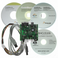
DEMO9S08EL32
Manufacturer Part Number
DEMO9S08EL32
Description
BOARD DEMO FOR 9S08 EL MCU
Manufacturer
Freescale Semiconductor
Type
MCUr
Datasheets
1.DEMO9S08EL32.pdf
(356 pages)
2.DEMO9S08EL32.pdf
(14 pages)
3.DEMO9S08EL32.pdf
(2 pages)
Specifications of DEMO9S08EL32
Contents
Evaluation Board
Processor To Be Evaluated
MC9S08EL32
Data Bus Width
8 bit
Interface Type
RS-232, USB
Operating Supply Voltage
12 V
Silicon Manufacturer
Freescale
Core Architecture
HCS08
Core Sub-architecture
HCS08
Silicon Core Number
MC9S08
Silicon Family Name
S08EL
Rohs Compliant
Yes
For Use With/related Products
MC9S08EL32
Lead Free Status / RoHS Status
Lead free / RoHS Compliant


Chapter 4 Memory
4.5.3
The FCDIV register must be initialized following any reset and any error flags cleared before beginning
command execution. The command execution steps are:
A partial command sequence can be aborted manually by writing a 0 to FCBEF any time after the write to
the memory array and before writing the 1 that clears FCBEF and launches the complete command.
Aborting a command in this way sets the FACCERR access error flag which must be cleared before
starting a new command.
A strictly monitored procedure must be obeyed or the command will not be accepted. This minimizes the
possibility of any unintended changes to the memory contents. The command complete flag (FCCF)
indicates when a command is complete. The command sequence must be completed by clearing FCBEF
to launch the command.
programming and sector erase abort.
48
1. Write a data value to an address in the FLASH or EEPROM array. The address and data
2. Write the command code for the desired command to FCMD. The six valid commands are blank
3. Write a 1 to the FCBEF bit in FSTAT to clear FCBEF and launch the command (including its
information from this write is latched into the FLASH and EEPROM interface. This write is a
required first step in any command sequence. For erase and blank check commands, the value of
the data is not important. For sector erase commands, the address can be any address in the
512-byte sector of FLASH or 8-byte sector of EEPROM to be erased. For mass erase and blank
check commands, the address can be any address in the FLASH or EEPROM memory. FLASH and
EEPROM erase independently of each other.
check (0x05), byte program (0x20), burst program (0x25), sector erase (0x40), mass erase (0x41),
and sector erase abort (0x47). The command code is latched into the command buffer.
address and data information).
Program and Erase Command Execution
1
Do not program any byte in the FLASH or EEPROM more than once after
a successful erase operation. Reprogramming bits in a byte which is already
programmed is not allowed without first erasing the sector in which the byte
resides or mass erasing the entire FLASH or EEPROM memory.
Programming without first erasing may disturb data stored in the FLASH or
EEPROM.
Excluding start/end overhead
Sector erase abort
Burst program
Byte program
Sector erase
Mass erase
Parameter
MC9S08EL32 Series and MC9S08SL16 Series Data Sheet, Rev. 3
Figure 4-2
Table 4-5. Program and Erase Times
is a flowchart for executing all of the commands except for burst
Cycles of FCLK
NOTE
20,000
4000
9
4
4
Time if FCLK = 200 kHz
100 ms
20 μs
20 μs
20 ms
45 μs
1
1
Freescale Semiconductor
Related parts for DEMO9S08EL32
Image
Part Number
Description
Manufacturer
Datasheet
Request
R

Part Number:
Description:
Manufacturer:
Freescale Semiconductor, Inc
Datasheet:
Part Number:
Description:
Manufacturer:
Freescale Semiconductor, Inc
Datasheet:
Part Number:
Description:
Manufacturer:
Freescale Semiconductor, Inc
Datasheet:
Part Number:
Description:
Manufacturer:
Freescale Semiconductor, Inc
Datasheet:
Part Number:
Description:
Manufacturer:
Freescale Semiconductor, Inc
Datasheet:
Part Number:
Description:
Manufacturer:
Freescale Semiconductor, Inc
Datasheet:
Part Number:
Description:
Manufacturer:
Freescale Semiconductor, Inc
Datasheet:
Part Number:
Description:
Manufacturer:
Freescale Semiconductor, Inc
Datasheet:
Part Number:
Description:
Manufacturer:
Freescale Semiconductor, Inc
Datasheet:
Part Number:
Description:
Manufacturer:
Freescale Semiconductor, Inc
Datasheet:
Part Number:
Description:
Manufacturer:
Freescale Semiconductor, Inc
Datasheet:
Part Number:
Description:
Manufacturer:
Freescale Semiconductor, Inc
Datasheet:
Part Number:
Description:
Manufacturer:
Freescale Semiconductor, Inc
Datasheet:
Part Number:
Description:
Manufacturer:
Freescale Semiconductor, Inc
Datasheet:
Part Number:
Description:
Manufacturer:
Freescale Semiconductor, Inc
Datasheet: