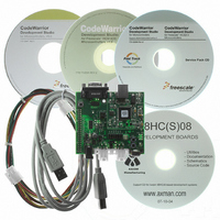
DEMO9S08EL32 Freescale Semiconductor, DEMO9S08EL32 Datasheet - Page 157

DEMO9S08EL32
Manufacturer Part Number
DEMO9S08EL32
Description
BOARD DEMO FOR 9S08 EL MCU
Manufacturer
Freescale Semiconductor
Type
MCUr
Datasheets
1.DEMO9S08EL32.pdf
(356 pages)
2.DEMO9S08EL32.pdf
(14 pages)
3.DEMO9S08EL32.pdf
(2 pages)
Specifications of DEMO9S08EL32
Contents
Evaluation Board
Processor To Be Evaluated
MC9S08EL32
Data Bus Width
8 bit
Interface Type
RS-232, USB
Operating Supply Voltage
12 V
Silicon Manufacturer
Freescale
Core Architecture
HCS08
Core Sub-architecture
HCS08
Silicon Core Number
MC9S08
Silicon Family Name
S08EL
Rohs Compliant
Yes
For Use With/related Products
MC9S08EL32
Lead Free Status / RoHS Status
Lead free / RoHS Compliant
- Current page: 157 of 356
- Download datasheet (9Mb)
10.4.7.2
If ADACK is selected as the conversion clock, the ADC continues operation during stop3 mode. For
guaranteed ADC operation, the MCU’s voltage regulator must remain active during stop3 mode. Consult
the module introduction for configuration information for this MCU.
If a conversion is in progress when the MCU enters stop3 mode, it continues until completion. Conversions
can be initiated while the MCU is in stop3 mode by means of the hardware trigger or if continuous
conversions are enabled.
A conversion complete event sets the COCO and generates an ADC interrupt to wake the MCU from stop3
mode if the ADC interrupt is enabled (AIEN = 1).
10.4.8
The ADC module is automatically disabled when the MCU enters either stop1 or stop2 mode. All module
registers contain their reset values following exit from stop1 or stop2. Therefore the module must be
re-enabled and re-configured following exit from stop1 or stop2.
10.5
This section gives an example which provides some basic direction on how a user would initialize and
configure the ADC module. The user has the flexibility of choosing between configuring the module for
8-bit or 10-bit resolution, single or continuous conversion, and a polled or interrupt approach, among many
other options. Refer to
10.5.1
10.5.1.1
Before the ADC module can be used to complete conversions, an initialization procedure must be
performed. A typical sequence is as follows:
Freescale Semiconductor
1. Update the configuration register (ADCCFG) to select the input clock source and the divide ratio
used to generate the internal clock, ADCK. This register is also used for selecting sample time and
low-power configuration.
Initialization Information
MCU Stop1 and Stop2 Mode Operation
ADC Module Initialization Example
Stop3 Mode With ADACK Enabled
Initialization Sequence
It is possible for the ADC module to wake the system from low power stop
and cause the MCU to begin consuming run-level currents without
generating a system level interrupt. To prevent this scenario, software
should ensure that the data transfer blocking mechanism (discussed in
Section 10.4.4.2, “Completing
and continuing ADC conversions.
Hexadecimal values designated by a preceding 0x, binary values designated
by a preceding %, and decimal values have no preceding character.
Table
MC9S08EL32 Series and MC9S08SL16 Series Data Sheet, Rev. 3
10-6,
Table
10-7, and
Conversions) is cleared when entering stop3
NOTE
NOTE
Table 10-8
for information used in this example.
Analog-to-Digital Converter (S08ADC10V1)
157
Related parts for DEMO9S08EL32
Image
Part Number
Description
Manufacturer
Datasheet
Request
R
Part Number:
Description:
Manufacturer:
Freescale Semiconductor, Inc
Datasheet:
Part Number:
Description:
Manufacturer:
Freescale Semiconductor, Inc
Datasheet:
Part Number:
Description:
Manufacturer:
Freescale Semiconductor, Inc
Datasheet:
Part Number:
Description:
Manufacturer:
Freescale Semiconductor, Inc
Datasheet:
Part Number:
Description:
Manufacturer:
Freescale Semiconductor, Inc
Datasheet:
Part Number:
Description:
Manufacturer:
Freescale Semiconductor, Inc
Datasheet:
Part Number:
Description:
Manufacturer:
Freescale Semiconductor, Inc
Datasheet:
Part Number:
Description:
Manufacturer:
Freescale Semiconductor, Inc
Datasheet:
Part Number:
Description:
Manufacturer:
Freescale Semiconductor, Inc
Datasheet:
Part Number:
Description:
Manufacturer:
Freescale Semiconductor, Inc
Datasheet:
Part Number:
Description:
Manufacturer:
Freescale Semiconductor, Inc
Datasheet:
Part Number:
Description:
Manufacturer:
Freescale Semiconductor, Inc
Datasheet:
Part Number:
Description:
Manufacturer:
Freescale Semiconductor, Inc
Datasheet:
Part Number:
Description:
Manufacturer:
Freescale Semiconductor, Inc
Datasheet:
Part Number:
Description:
Manufacturer:
Freescale Semiconductor, Inc
Datasheet:


