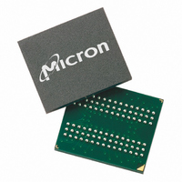
MT48H8M32LFB5-10 Micron Technology Inc, MT48H8M32LFB5-10 Datasheet - Page 29

MT48H8M32LFB5-10
Manufacturer Part Number
MT48H8M32LFB5-10
Description
IC SDRAM 256MBIT 100MHZ 90VFBGA
Manufacturer
Micron Technology Inc
Datasheet
1.MT48V8M32LFB5-8_IT_TR.pdf
(75 pages)
Specifications of MT48H8M32LFB5-10
Format - Memory
RAM
Memory Type
Mobile SDRAM
Memory Size
256M (8Mx32)
Speed
100MHz
Interface
Parallel
Voltage - Supply
1.7 V ~ 1.95 V
Operating Temperature
0°C ~ 70°C
Package / Case
90-VFBGA
Lead Free Status / RoHS Status
Lead free / RoHS Compliant
Available stocks
Company
Part Number
Manufacturer
Quantity
Price
Company:
Part Number:
MT48H8M32LFB5-10
Manufacturer:
MICRON
Quantity:
10 000
Company:
Part Number:
MT48H8M32LFB5-10
Manufacturer:
Micron Technology Inc
Quantity:
10 000
Company:
Part Number:
MT48H8M32LFB5-10 IT
Manufacturer:
Micron Technology Inc
Quantity:
10 000
Company:
Part Number:
MT48H8M32LFB5-10 IT TR
Manufacturer:
Micron Technology Inc
Quantity:
10 000
Company:
Part Number:
MT48H8M32LFB5-10 TR
Manufacturer:
Micron Technology Inc
Quantity:
10 000
Company:
Part Number:
MT48H8M32LFB5-10IT
Manufacturer:
MICRON
Quantity:
20 000
Figure 14: READ to PRECHARGE
PDF: 09005aef80d460f2/Source: 09005aef80cd8d41
256Mb SDRAM x32_2.fm - Rev. G 6/05
Note:
Full-page READ bursts can be truncated with the BURST TERMINATE command, and
fixed-length READ bursts may be truncated with a BURST TERMINATE command, pro-
vided that auto precharge was not activated. The BURST TERMINATE command should
be issued x cycles before the clock edge at which the last desired data element is valid,
where x equals the CAS latency minus one. This is shown in Figure 15 for each possible
CAS latency; data element n + 3 is the last desired data element of a longer burst.
DQM is LOW.
COMMAND
COMMAND
COMMAND
ADDRESS
ADDRESS
ADDRESS
CLK
CLK
CLK
DQ
DQ
DQ
BANK a,
BANK a,
BANK a,
COL n
T0
T0
COL n
T0
COL n
READ
READ
READ
CL = 1
CL = 2
T1
T1
T1
NOP
NOP
NOP
D
OUT
CL = 3
n
29
T2
T2
T2
NOP
NOP
NOP
D
D
n + 1
OUT
OUT
n
Micron Technology, Inc., reserves the right to change products or specifications without notice.
T3
T3
T3
NOP
NOP
NOP
D
n + 2
D
D
n + 1
OUT
OUT
OUT
n
PRECHARGE
PRECHARGE
PRECHARGE
(a or all)
(a or all)
(a or all)
T4
BANK
T4
BANK
BANK
T4
X = 0 cycles
X = 1 cycle
D
n + 3
D
n + 2
D
n + 1
256Mb: x32 Mobile SDRAM
OUT
OUT
OUT
X = 2 cycles
T5
T5
T5
NOP
NOP
NOP
D
n + 2
D
n + 3
OUT
OUT
t RP
t RP
t RP
©2003 Micron Technology, Inc. All rights reserved.
T6
T6
T6
NOP
NOP
NOP
D
n + 3
OUT
DON’T CARE
BANK a,
BANK a,
BANK a,
ACTIVE
ACTIVE
ACTIVE
T7
T7
T7
Operation
ROW
ROW
ROW


